参数资料
| 型号: | MAX17498AATE+T |
| 厂商: | Maxim Integrated |
| 文件页数: | 10/20页 |
| 文件大小: | 0K |
| 描述: | IC OFF-LINE CONVERTER 16TQFN |
| 产品培训模块: | Obsolescence Mitigation Program |
| 标准包装: | 2,500 |
| 输出隔离: | 隔离 |
| 频率范围: | 235kHz ~ 265kHz |
| 输入电压: | 4.5 V ~ 29 V |
| 工作温度: | -40°C ~ 125°C |
| 封装/外壳: | 16-WFQFN 裸露焊盘 |
| 供应商设备封装: | 16-TQFN-EP(3x3) |
| 包装: | 带卷 (TR) |
�� �
�
�MAX17498A/MAX17498B/MAX17498C�
�AC-DC� and� DC-DC� Peak� Current-Mode� Converters�
�for� Flyback/Boost� Applications�
�Configuring� the� Power� Stage� (LX)�
�The� devices� use� an� internal� n-channel� MOSFET� to� imple-�
�ment� internal� current� sensing� for� current-mode� control� and�
�overcurrent� protection� of� the� flyback/boost� converter.� To�
�facilitate� this,� the� drain� of� the� internal� nMOSFET� is� connect-�
�ed� to� the� source� of� the� external� MOSFET� in� the� MAX17498A�
�high-input-voltage� applications.� The� gate� of� the� external�
�MOSFET� is� connected� to� the� IN� pin.� Ensure� by� design� that�
�the� IN� pin� voltage� does� not� exceed� the� maximum� operating�
�gate-voltage� rating� of� the� external� MOSFET.� The� external�
�MOSFET� gate-source� voltage� is� controlled� by� the� switch-�
�ing� action� of� the� internal� nMOSFET,� while� also� sensing� the�
�source� current� of� the� external� MOSFET.� In� the� MAX17498B/�
�MAX17498C-based� applications,� the� LX� pin� is� directly� con-�
�nected� to� either� the� flyback� transformer� primary� winding� or�
�to� the� boost-converter� inductor.�
�IN�
�10μA�
�Maximum� Duty� Cycle�
�The� MAX17498A/MAX17498C� operate� at� a� maximum�
�duty� cycle� of� 94%.� The� MAX17498B� offers� a� maximum�
�duty� cycle� of� 92%.� The� devices� can� be� used� to� imple-�
�ment� flyback� and� boost� converters� involving� large� input-�
�to-output� voltage� ratios� in� DC-DC� applications.�
�Power-Good� Signal� (PGOOD)�
�The� devices� include� a� PGOOD� signal� that� serves� as�
�a� power-good� signal� to� the� system.� PGOOD� is� an�
�open-drain� signal� and� requires� a� pullup� resistor� to� the�
�preferred� supply� voltage.� The� PGOOD� signal� monitors�
�EA-� and� pulls� high� when� EA-� is� 95%� (typ)� of� its� regulation�
�value� (1.22V).� For� isolated� power� supplies,� PGOOD� can-�
�not� serve� as� a� power-good� signal.�
�REF�
�SSDONE�
�SSDONE�
�VOLTAGE� SS�
�CHIPEN�
�HICCUP�
�SS�
�V� CC�
�5V,� 50mA�
�POK�
�LDO�
�33V� CLAMP�
�(MAX17498A� ONLY)�
�BG�
�SS�
�CURRENT� SS�
�MAX17498A�
�MAX17498B�
�MAX17498C�
�1.17V�
�SSDONEF�
�EN/UVLO�
�OVI�
�1.23V�
�1.23V�
�V� CS�
�CHIPEN�
�OSC�
�RUNAWAY�
�CLK�
�V� SLOPE�
�V� SUM�
�1� RUNAWAY�
�V� CS�
�SSDONE�
�LX�
�LIM�
�10μA�
�1.23V�
�LIMINT�
�V� SUM�
�PEAK�
�PWM�
�CONTROL�
�LOGIC� AND�
�DRIVER�
�PGOOD�
�PGND�
�PGOOD�
�SLOPE�
�10μA�
�250mV�
�DECODER�
�COMP�
�FIXED� SLOPE�
�VARIABLE� SLOPE�
�EA-�
�BLOCK�
�COMP�
�EA+�
�EA-�
�VOLTAGE� SS� CURRENT� SS�
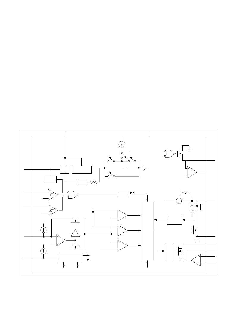
�Figure� 1.� MAX17498A/MAX17498B/MAX17498C� Block� Diagram�
�Maxim� Integrated�
�CHIPEN�
�10�
�相关PDF资料 |
PDF描述 |
|---|---|
| MAX17500BEUB+ | IC REG CTRLR BST ISO PWM 10-UMAX |
| MAX17510ATB+T | IC REG DDR LOW VOLTAGE 10-TDFN |
| MAX17528GTJ+T | IC CTLR PWM VID PS 1PH 32-TQFN |
| MAX17535ETG+T | IC SMBUS BATT CHARGER 24TQFN |
| MAX1757EAI+T | IC BATTERY CHRG LI+ 28-SSOP |
相关代理商/技术参数 |
参数描述 |
|---|---|
| MAX17498BATE+ | 功能描述:电流型 PWM 控制器 Univ AC/DC-Iso DC/DC Flyback controller RoHS:否 制造商:Texas Instruments 开关频率:27 KHz 上升时间: 下降时间: 工作电源电压:6 V to 15 V 工作电源电流:1.5 mA 输出端数量:1 最大工作温度:+ 105 C 安装风格:SMD/SMT 封装 / 箱体:TSSOP-14 |
| MAX17498BATE+CER | 功能描述:直流/直流开关转换器 ACDC & DCDC Peak Crnt-Mode Cnvtrs RoHS:否 制造商:STMicroelectronics 最大输入电压:4.5 V 开关频率:1.5 MHz 输出电压:4.6 V 输出电流:250 mA 输出端数量:2 最大工作温度:+ 85 C 安装风格:SMD/SMT |
| MAX17498BATE+T | 功能描述:电流型 PWM 控制器 MAX17498BATE+T RoHS:否 制造商:Texas Instruments 开关频率:27 KHz 上升时间: 下降时间: 工作电源电压:6 V to 15 V 工作电源电流:1.5 mA 输出端数量:1 最大工作温度:+ 105 C 安装风格:SMD/SMT 封装 / 箱体:TSSOP-14 |
| MAX17498BATE+TCER | 功能描述:直流/直流开关转换器 Universal ACDC & Iso DCDC Flyback cntlr RoHS:否 制造商:STMicroelectronics 最大输入电压:4.5 V 开关频率:1.5 MHz 输出电压:4.6 V 输出电流:250 mA 输出端数量:2 最大工作温度:+ 85 C 安装风格:SMD/SMT |
| MAX17498BEVKIT# | 功能描述:电源管理IC开发工具 MAX17498 Eval Kit RoHS:否 制造商:Maxim Integrated 产品:Evaluation Kits 类型:Battery Management 工具用于评估:MAX17710GB 输入电压: 输出电压:1.8 V |
发布紧急采购,3分钟左右您将得到回复。