- 您现在的位置:买卖IC网 > PDF目录15036 > MAX1771EPA (Maxim Integrated Products)IC REG CTRLR BST PWM 8-DIP PDF资料下载
参数资料
| 型号: | MAX1771EPA |
| 厂商: | Maxim Integrated Products |
| 文件页数: | 13/16页 |
| 文件大小: | 0K |
| 描述: | IC REG CTRLR BST PWM 8-DIP |
| 产品培训模块: | Lead (SnPb) Finish for COTS Obsolescence Mitigation Program |
| 标准包装: | 50 |
| PWM 型: | 控制器 |
| 输出数: | 1 |
| 频率 - 最大: | 500kHz |
| 占空比: | 92% |
| 电源电压: | 3 V ~ 16.5 V |
| 降压: | 无 |
| 升压: | 是 |
| 回扫: | 无 |
| 反相: | 无 |
| 倍增器: | 无 |
| 除法器: | 无 |
| Cuk: | 无 |
| 隔离: | 无 |
| 工作温度: | -40°C ~ 85°C |
| 封装/外壳: | 8-DIP(0.300",7.62mm) |
| 包装: | 管件 |
�� �
�
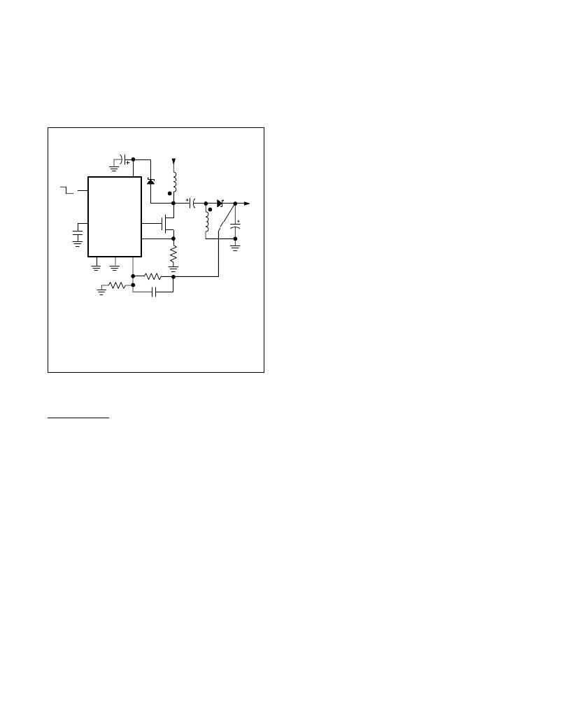
�MAX1771�
�12V� or� Adjustable,� High-Efficiency,�
�Low� I� Q� ,� Step-Up� DC-DC� Controller�
�Layout� Considerations�
�1N5817�
�3V� =� OFF�
�4�
�SHDN�
�C1�
�2.2� μ� F�
�V+�
�2�
�D2�
�V� IN� *�
�3V� TO� 11V�
�L1�
�20� μ� H�
�1� CTX20-4�
�D1�
�1N5817�
�V� OUT�
�5V�
�500mA�
�Due� to� high� current� levels� and� fast� switching� wave-�
�forms,� which� radiate� noise,� proper� PC� board� layout� is�
�essential.� Protect� sensitive� analog� grounds� by� using� a�
�star� ground� configuration.� Minimize� ground� noise� by�
�connecting� GND,� the� input� bypass� capacitor� ground�
�lead,� and� the� output� filter� capacitor� ground� lead� to� a�
�single� point� (star� ground� configuration).� Also,� minimize�
�C4� 5�
�0.1� μ� F�
�REF�
�MAX1771�
�EXT�
�CS�
�1�
�8�
�C2�
�Q1**� 47� μ� F�
�16V�
�L2�
�C3�
�220� μ� F�
�10V�
�lead� lengths� to� reduce� stray� capacitance,� trace� resis-�
�tance,� and� radiated� noise.� Place� input� bypass� capaci-�
�tor� C2� as� close� as� possible� to� V+� and� GND.�
�Excessive� noise� at� the� V+� input� may� falsely� trigger� the�
�GND� AGND�
�7� 6�
�R2� ?�
�FB�
�3�
�R3� ?�
�R1�
�0.1� ?�
�timing� circuitry,� resulting� in� short� pulses� at� EXT.� If� this�
�occurs� it� will� have� a� negligible� effect� on� circuit� efficien-�
�cy.� If� desired,� place� a� 4.7μF� directly� across� the� V+� and�
�GND� pins� (in� parallel� with� the� 0.1μF� C2� bypass� capaci-�
�tor)� to� reduce� the� noise� at� V+.�
�C5�
�47pF�
�SEE� TEXT� FOR� FURTHER� COMPONENT� INFO�
�*� *� V� IN� MAY� BE� LOWER� THAN� INDICATED� IF� THE� SUPPLY� IS� NOT�
�**� REQUIRED� TO� START� UNDER� FULL� LOAD�
�**MOTOROLA� MMFT3055ELT1�
�?� FOR� 5V:� R2� =� 200k� ?� ,� R3� =� 470k� ?�
�3.3V:� R2� =� 100k� ?� ,� R3� =� 20k� ?�
�Figure� 5.� Step-Up/Down� for� a� 5V/3.3V� Output�
�Applications� Information�
�Low� Input� Voltage� Operation�
�When� using� a� power� supply� that� decays� with� time�
�(such� as� a� battery),� the� N-FET� transistor� will� operate� in�
�its� linear� region� when� the� voltage� at� EXT� approaches�
�the� threshold� voltage� of� the� FET,� dissipating� excessive�
�power.� Prolonged� operation� in� this� mode� may� damage�
�the� FET.� This� effect� is� much� more� significant� in� non-�
�bootstrapped� mode� than� in� bootstrapped� mode,� since�
�bootstrapped� mode� typically� provides� much� higher�
�V� GS� voltages.� To� avoid� this� condition,� make� sure� V� EXT�
�is� above� the� V� TH� of� the� FET,� or� use� a� voltage� detector�
�(such� as� the� MAX8211)� to� put� the� IC� in� shutdown� mode�
�once� the� input� supply� voltage� falls� below� a� predeter-�
�mined� minimum� value.� Excessive� loads� with� low� input�
�voltages� can� also� cause� this� condition.�
�Starting� Up� Under� Load�
�The� Typical� Operating� Characteristics� show� the� Start-�
�Up� Voltage� vs.� Load� Current� graph� for� bootstrapped-�
�mode� operation.� This� graph� depends� on� the� type�
�of� power� switch� used.� The� MAX1771� is� not� designed� to�
�start� up� under� full� load� in� bootstrapped� mode� with� low�
�input� voltages.�
�Maxim� Integrated�
�Other� Application� Circuits�
�4� Cells� to� 5V� (or� 3� Cells� to� 3.3V),� 500mA�
�Step-Up/Down� Converter�
�The� circuit� shown� in� Figure� 5� generates� 5V� (or� 3.3V)� at�
�500mA� with� 85%� efficiency,� from� an� input� voltage� that�
�varies� above� and� below� the� output.� The� output� couples�
�to� the� switching� circuitry� via� a� capacitor.� This� configu-�
�ration� offers� two� advantages� over� flyback-transformer�
�and� step-up� linear-regulator� circuits:� smooth� regulation�
�as� the� input� passes� through� the� output,� and� no� output�
�current� in� shutdown.�
�This� circuit� requires� two� inductors,� which� can� be� wound�
�on� one� core� with� no� regard� to� coupling� since� they� do�
�not� work� as� a� transformer.� L1� and� L2� can� either� be�
�wound� together� (as� with� the� Coiltronics� CTX20-4)� or�
�kept� as� two� separate� inductors;� both� methods� provide�
�equal� performance.� Capacitors� C2� and� C3� should� be�
�low-ESR� types� for� best� efficiency.� A� 1μF� ceramic�
�capacitor� will� work� at� C2,� but� with� about� 3%� efficiency�
�loss.� C2’s� voltage� rating� must� be� greater� than� the� maxi-�
�mum� input� voltage.� Also� note� that� the� LX� switch� must�
�withstand� a� voltage� equal� to� the� sum� of� the� input� and�
�output� voltage;� for� example,� when� converting� 11V� to�
�5V,� the� switch� must� withstand� 16V.�
�LX� switch� pulses� are� captured� by� Schottky� diode� D2� to�
�boost� V+� to� (V� OUT� +� V� IN� ).� This� improves� efficiency� with�
�a� low� input� voltage,� but� also� limits� the� maximum� input�
�supply� to� 11V.� If� the� input� voltage� does� not� fall� below� 4V�
�and� if� a� 3V� logic� threshold� FET� is� used� for� Q1,� you� may�
�omit� D2� and� connect� V+� directly� to� the� input� supply.�
�12V� Output� Buck/Boost�
�The� circuit� in� Figure� 6� generates� 12V� from� a� 4.5V� to�
�16V� input.� Higher� input� voltages� are� possible� if� you�
�13�
�相关PDF资料 |
PDF描述 |
|---|---|
| VI-JWX-EW-F2 | CONVERTER MOD DC/DC 5.2V 100W |
| DS1233D-10 | IC ECONORESET NO PBR 10% TO92-3 |
| B43088A5226M | 22UF 450V 16X25 SINGLE END |
| VI-JWV-EW-F1 | CONVERTER MOD DC/DC 5.8V 100W |
| VI-JW0-EW-F3 | CONVERTER MOD DC/DC 5V 100W |
相关代理商/技术参数 |
参数描述 |
|---|---|
| MAX1771EPA+ | 功能描述:DC/DC 开关控制器 12/Adj V Low IQ Step-Up RoHS:否 制造商:Texas Instruments 输入电压:6 V to 100 V 开关频率: 输出电压:1.215 V to 80 V 输出电流:3.5 A 输出端数量:1 最大工作温度:+ 125 C 安装风格: 封装 / 箱体:CPAK |
| MAX1771ESA | 功能描述:DC/DC 开关控制器 12/Adj V Low IQ Step-Up RoHS:否 制造商:Texas Instruments 输入电压:6 V to 100 V 开关频率: 输出电压:1.215 V to 80 V 输出电流:3.5 A 输出端数量:1 最大工作温度:+ 125 C 安装风格: 封装 / 箱体:CPAK |
| MAX1771ESA+ | 功能描述:DC/DC 开关控制器 12/Adj V Low IQ Step-Up RoHS:否 制造商:Texas Instruments 输入电压:6 V to 100 V 开关频率: 输出电压:1.215 V to 80 V 输出电流:3.5 A 输出端数量:1 最大工作温度:+ 125 C 安装风格: 封装 / 箱体:CPAK |
| MAX1771ESA+T | 功能描述:DC/DC 开关控制器 12/Adj V Low IQ Step-Up RoHS:否 制造商:Texas Instruments 输入电压:6 V to 100 V 开关频率: 输出电压:1.215 V to 80 V 输出电流:3.5 A 输出端数量:1 最大工作温度:+ 125 C 安装风格: 封装 / 箱体:CPAK |
| MAX1771ESA-T | 功能描述:DC/DC 开关控制器 12/Adj V Low IQ Step-Up RoHS:否 制造商:Texas Instruments 输入电压:6 V to 100 V 开关频率: 输出电压:1.215 V to 80 V 输出电流:3.5 A 输出端数量:1 最大工作温度:+ 125 C 安装风格: 封装 / 箱体:CPAK |
发布紧急采购,3分钟左右您将得到回复。