- 您现在的位置:买卖IC网 > PDF目录13110 > MAX1778EUG+ (Maxim Integrated Products)IC DCDC CONV MULTI OUT 24TSSOP PDF资料下载
参数资料
| 型号: | MAX1778EUG+ |
| 厂商: | Maxim Integrated Products |
| 文件页数: | 32/39页 |
| 文件大小: | 0K |
| 描述: | IC DCDC CONV MULTI OUT 24TSSOP |
| 产品培训模块: | Lead (SnPb) Finish for COTS Obsolescence Mitigation Program |
| 标准包装: | 62 |
| 应用: | 转换器,TFT,LCD |
| 输入电压: | 2.7 V ~ 5.5 V |
| 输出数: | 5 |
| 输出电压: | 2.7 V ~ 13 V |
| 工作温度: | 0°C ~ 85°C |
| 安装类型: | 表面贴装 |
| 封装/外壳: | 24-TSSOP(0.173",4.40mm 宽) |
| 供应商设备封装: | 24-TSSOP |
| 包装: | 管件 |
第1页第2页第3页第4页第5页第6页第7页第8页第9页第10页第11页第12页第13页第14页第15页第16页第17页第18页第19页第20页第21页第22页第23页第24页第25页第26页第27页第28页第29页第30页第31页当前第32页第33页第34页第35页第36页第37页第38页第39页
�� �
�
�MAX1778/MAX1880–MAX1885�
�Quad-Output� TFT� LCD� DC/DC�
�Converters� with� Buffer�
�layer� boards,� the� top� layer� should� contain� the� boost�
�regulator� and� charge-pump� power� ground� plane,�
�and� the� inner� layer� should� contain� the� analog�
�ground� plane� and� power-ground� plane/path� for� the�
�VCOM� buffer� and� LDO.� Connect� all� three� ground�
�planes� together� at� one� place� near� the� PGND� pin.�
�3)� Locate� all� feedback� resistive-dividers� as� close� as�
�possible� to� their� respective� feedback� pins.� The� volt-�
�age-divider’s� center� trace� should� be� kept� short.�
�Avoid� running� any� feedback� trace� near� the� LX�
�switching� node� or� the� charge-pump� drivers.� The�
�resistive-dividers’� ground� connections� should� be� to�
�analog� ground� (GND).�
�4)� When� using� multilayer� boards,� separate� the� top� sig-�
�nal� layer� and� bottom� signal� layer� with� a� ground�
�plane� between� to� eliminate� capacitive� coupling�
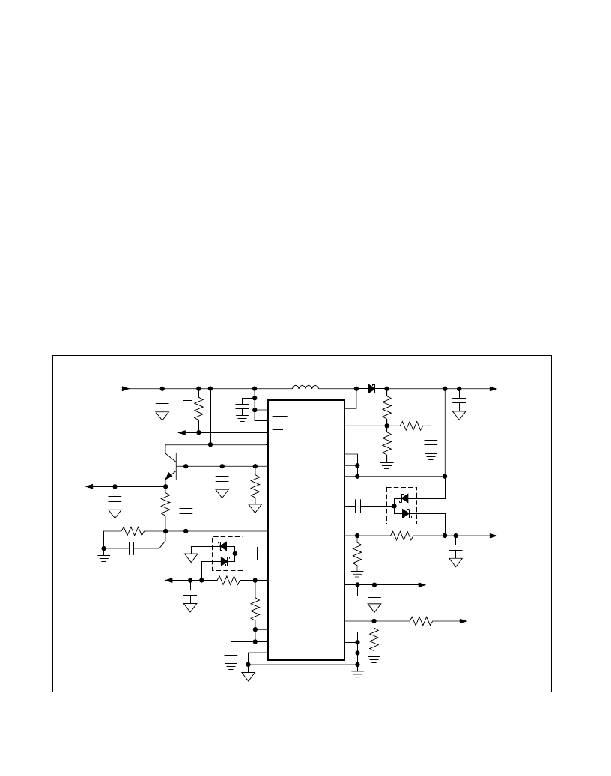
�L1�
�between� fast-charging� nodes� on� the� top� layer� and�
�high-impedance� nodes� on� the� bottom� layer.� The�
�fast-charging� nodes,� such� as� the� LX� and� charge-�
�pump� driver� nodes,� should� not� have� any� other�
�traces� or� ground� planes� near� by.�
�5)� Keep� the� charge-pump� circuitry� as� close� as� possi-�
�ble� to� the� IC,� using� wide� traces� and� avoiding� vias�
�when� possible.� Place� 0.1μF� ceramic� bypass�
�capacitors� near� the� charge-pump� input� pins� (SUPP�
�and� SUPN)� to� the� PGND� pin.�
�6)� To� maximize� output� power� and� efficiency� and� mini-�
�mize� output� ripple� voltage,� use� extra-wide,� power-�
�ground� traces,� and� solder� the� IC’s� power-ground�
�pin� directly� to� it.�
�Refer� to� the� MAX1778/MAX1880–MAX1885� evaluation�
�kit� for� an� example� of� proper� board� layout.�
�INPUT�
�10� μ� H�
�MAIN�
�V� IN� =� 5V�
�C� IN�
�(2)� 4.7� μ� F�
�R� RDY�
�100k� ?�
�C1�
�0.22� μ� F�
�IN�
�SHDN�
�LX�
�FB�
�R1�
�86.6k� ?�
�R� COMP�
�4.7k� ?�
�C� OUT�
�(2)� 10� μ� F�
�V� MAIN� =� 12V�
�TO� LOGIC�
�RDY�
�SUPL�
�SUPB�
�R2�
�10k� ?�
�C� COMP�
�470pF�
�LDO�
�V� LDO� =� 3.3V�
�C6�
�1� μ� F�
�R8�
�10k� ?�
�Q1�
�R7�
�16.4k� ?�
�C� LDOOUT�
�4.7� μ� F�
�C6�
�0.01� μ� F�
�R8�
�1.5k� ?�
�LDOOUT�
�MAX1778�
�SUPN�
�SUPP�
�DRVP�
�C4�
�0.1� μ� F�
�750k� ?�
�C7�
�0.01� μ� F�
�NEGATIVE�
�V� NEG� =� -8V�
�C3�
�1.0� μ� F�
�C2�
�0.1� μ� F�
�R5�
�316k� ?�
�R6�
�49.9k� ?�
�FBL�
�DRVN�
�FBN�
�FBP�
�BUFOUT�
�BUF-�
�FLTSET�
�R4�
�49.9k� ?�
�C� BUF�
�1.0� μ� F�
�R3�
�R9�
�30k� ?�
�C5�
�1.0� μ� F�
�BUFFER� OUTPUT�
�V� BUFOUT� =� V� SUPB� /2�
�REF�
�POSITIVE�
�V� POS� =� 20V�
�C� REF�
�0.22� μ� F�
�REF�
�INTG�
�PGND�
�BUF+�
�GND�
�TGND�
�R10�
�100k� ?�
�Figure� 8.� 5V� Input� Monitor� Application�
�32�
�Maxim� Integrated�
�相关PDF资料 |
PDF描述 |
|---|---|
| MAX5008CUB+ | IC CHARGE PUMP USB 5V 10-UMAX |
| VI-2W4-EW-B1 | CONVERTER MOD DC/DC 48V 100W |
| RBM36DTMS | CONN EDGECARD 72POS R/A .156 SLD |
| 500R15W104KV4T | CAP CER 0.1UF 50V 10% X7R 0805 |
| RCM40DTMH | CONN EDGECARD 80POS R/A .156 SLD |
相关代理商/技术参数 |
参数描述 |
|---|---|
| MAX1778EUG+ | 功能描述:直流/直流开关转换器 Quad-Output TFT LCD w/Buffer RoHS:否 制造商:STMicroelectronics 最大输入电压:4.5 V 开关频率:1.5 MHz 输出电压:4.6 V 输出电流:250 mA 输出端数量:2 最大工作温度:+ 85 C 安装风格:SMD/SMT |
| MAX1778EUG+T | 功能描述:直流/直流开关转换器 Quad-Output TFT LCD w/Buffer RoHS:否 制造商:STMicroelectronics 最大输入电压:4.5 V 开关频率:1.5 MHz 输出电压:4.6 V 输出电流:250 mA 输出端数量:2 最大工作温度:+ 85 C 安装风格:SMD/SMT |
| MAX1778EUG-T | 功能描述:直流/直流开关转换器 RoHS:否 制造商:STMicroelectronics 最大输入电压:4.5 V 开关频率:1.5 MHz 输出电压:4.6 V 输出电流:250 mA 输出端数量:2 最大工作温度:+ 85 C 安装风格:SMD/SMT |
| MAX1778EVKIT | 功能描述:电源管理IC开发工具 MAX1778/80/81/82 Eval Kit RoHS:否 制造商:Maxim Integrated 产品:Evaluation Kits 类型:Battery Management 工具用于评估:MAX17710GB 输入电压: 输出电压:1.8 V |
| MAX1779EUE | 功能描述:直流/直流开关转换器 RoHS:否 制造商:STMicroelectronics 最大输入电压:4.5 V 开关频率:1.5 MHz 输出电压:4.6 V 输出电流:250 mA 输出端数量:2 最大工作温度:+ 85 C 安装风格:SMD/SMT |
发布紧急采购,3分钟左右您将得到回复。