- 您现在的位置:买卖IC网 > PDF目录19809 > MAX1793EUE18+T (Maxim Integrated)IC REG LDO 1.8V/ADJ 1A 16TSSOP PDF资料下载
参数资料
| 型号: | MAX1793EUE18+T |
| 厂商: | Maxim Integrated |
| 文件页数: | 9/11页 |
| 文件大小: | 0K |
| 描述: | IC REG LDO 1.8V/ADJ 1A 16TSSOP |
| 产品培训模块: | Lead (SnPb) Finish for COTS Obsolescence Mitigation Program |
| 标准包装: | 2,500 |
| 稳压器拓扑结构: | 正,固定式或可调式 |
| 输出电压: | 1.8V,1.25 V ~ 5 V |
| 输入电压: | 2.5 V ~ 5.5 V |
| 稳压器数量: | 1 |
| 电流 - 输出: | 1A(最小) |
| 工作温度: | -40°C ~ 85°C |
| 安装类型: | 表面贴装 |
| 封装/外壳: | 16-TSSOP(0.173",4.40mm)裸露焊盘 |
| 供应商设备封装: | 16-TSSOP-EP |
| 包装: | 带卷 (TR) |
�� �
�
�Low-Dropout,� Low� I� Q� ,� 1A� Linear� Regulator�
�Thermal-overload� protection� is� designed� to� safeguard�
�the� MAX1793� in� the� event� of� fault� conditions.� For� con-�
�tinuous� operation,� do� not� exceed� the� absolute� maxi-�
�mum� junction-temperature� rating� of� T� J� =� +150°C.�
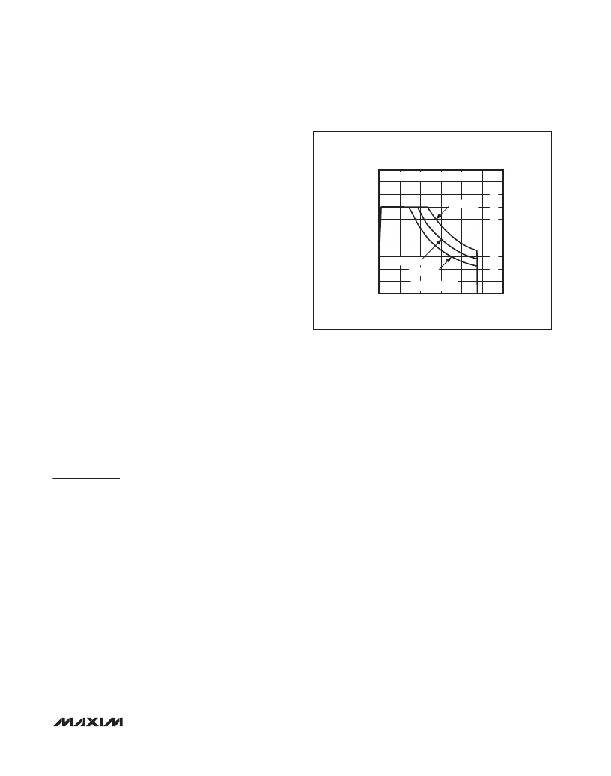
�Operating� Region� and� Power� Dissipation�
�Maximum� power� dissipation� of� the� MAX1793� depends�
�on� the� thermal� resistance� of� the� case� and� circuit� board,�
�the� temperature� difference� between� the� die� junction�
�and� ambient� air,� and� the� rate� of� air� flow.� The� power� dis-�
�sipated� by� the� device� is:� P� =� I� OUT� (V� IN� –� V� OUT� ).� The�
�resulting� maximum� power� dissipation� is:�
�P� MAX� =� [(T� J(MAX)� –� T� A� )/(� θ� JC� +� θ� CA� )]�
�2.0�
�1.8�
�1.6�
�1.4�
�1.2�
�1.0�
�0.8�
�0.6�
�0.4�
�MAXIMUM� OUTPUT� CURRENT� vs.�
�INPUT-OUTPUT� DIFFERENTIAL� VOLTAGE�
�MAXIMUM CONTINUOUS CURRENT�
�T� A� = +25°C�
�T� A� = +50°C�
�T� A� = +70°C�
�where� (T� J(MAX)� –� T� A� )� is� the� temperature� difference�
�between� the� maximum� allowed� die� junction� (+150°C)� and�
�the� surrounding� air,� θ� JC� (junction-to-case)� is� the� thermal�
�resistance� of� the� package� chosen,� and� θ� CA� is� the� thermal�
�0.2�
�0�
�0�
�T� J(MAX)� = +150°C�
�1� 2� 3� 4� 5�
�INPUT-OUTPUT� DIFFERENTIAL� VOLTAGE� (V)�
�6�
�resistance� from� the� case� through� the� PCB,� copper� traces,�
�and� other� materials� to� the� surrounding� air.� Figure� 4� shows�
�allowable� power� dissipation� for� typical� PCBs� at� +25°C,�
�+50°C,� and� +70°C� ambient� temperatures.�
�The� MAX1793� TSSOP-EP� package� features� an� exposed�
�thermal� pad� on� its� underside.� This� pad� lowers� the� ther-�
�mal� resistance� of� the� package� by� providing� a� direct� heat�
�conduction� path� from� the� die� to� the� PCB.� Additionally,�
�the� ground� pin� (GND)� also� channels� heat.� Connect� the�
�exposed� thermal� pad� and� GND� to� circuit� ground� by�
�using� a� large� pad� (minimum� 1in� 2� recommended),� or� mul-�
�tiple� vias� to� the� ground� plane.�
�Applications� Information�
�Capacitor� Selection�
�and� Regulator� Stability�
�Capacitors� are� required� at� the� input� and� output� of� the�
�MAX1793.� Connect� a� 4.7μF� capacitor� between� IN� and�
�ground� (C� IN� )� and� a� 6.8μF� capacitor� between� OUT� and�
�ground� (C� OUT� ).� C� IN� serves� only� to� lower� the� source�
�impedance� of� the� input� supply� and� may� be� smaller� than�
�4.7μF� when� the� MAX1793� is� powered� from� regulated�
�power� supplies� or� low-impedance� batteries.�
�The� output� capacitor’s� equivalent� series� resistance� (ESR)�
�affects� stability� and� output� noise.� C� OUT� ESR� should� be�
�0.5� ?� or� less� to� ensure� stability� and� optimum� transient�
�response.� Surface-mount� ceramic� capacitors� have� very�
�low� ESR� and� are� commonly� available� in� values� up� to�
�10μF.� Other� low-ESR� (<� 0.5� ?� )� capacitors,� such� as� sur-�
�face-mount� tantalum� or� OS-CON,� may� also� be� used.�
�Connect� CIN� and� C� OUT� as� close� to� the� IC� as� possible� to�
�minimize� the� impact� of� PCB� trace� inductance.�
�Figure� 4.� Power� Operating� Region:� Maximum� Output� Current�
�vs.� Input-Output� Differential� Voltage�
�Noise,� PSRR,� and� Transient� Response�
�The� MAX1793� output� noise� is� typically� 115μV� RMS� during�
�normal� operation.� This� is� suitably� low� for� most� applica-�
�tions.� See� the� output� noise� plot� in� the� Typical� Operating�
�Characteristics.�
�The� MAX1793� is� designed� to� achieve� low� dropout� volt-�
�age� and� low� quiescent� current� in� battery-powered� sys-�
�tems� while� still� maintaining� good� noise,� transient�
�response,� and� AC� rejection.� See� the� Typical� Operating�
�Characteristics� for� a� plot� of� Power-Supply� Rejection�
�Ratio� (PSRR)� vs.� Frequency.� When� operating� from� very�
�noisy� sources,� supply� noise� rejection� and� transient�
�response� can� be� improved� by� increasing� the� values� of�
�the� input� and� output� capacitors� and� employing� passive�
�postfiltering.�
�Input-Output� (Dropout)� Voltage�
�A� regulator’s� minimum� input-to-output� voltage� differential�
�(dropout� voltage)� determines� the� lowest� usable� supply�
�voltage.� In� battery-powered� systems,� this� determines� the�
�useful� end-of-life� battery� voltage.� Since� a� p-channel�
�MOSFET� is� used� as� the� pass� device,� dropout� voltage� is�
�the� product� of� R� DS(ON)� and� load� current� (see� the�
�Electrical� Characteristics� and� Dropout� Voltage� vs.� Load�
�Current� in� the� Typical� Operating� Characteristics).� The�
�MAX1793� operating� current� typically� remains� below�
�225μA� in� dropout.�
�_______________________________________________________________________________________�
�9�
�相关PDF资料 |
PDF描述 |
|---|---|
| 5-641285-2 | 22 CIR MTA 156 EDG CON F/T LF |
| VI-B7M-CY-F3 | CONVERTER MOD DC/DC 10V 50W |
| VE-J4X-CW-B1 | CONVERTER MOD DC/DC 5.2V 100W |
| MAX1806EUA18+T | IC REG LDO 1.8V/ADJ .5A 8-UMAX |
| EEM24DSES-S243 | CONN EDGECARD 48POS .156 EYELET |
相关代理商/技术参数 |
参数描述 |
|---|---|
| MAX1793EUE20 | 功能描述:低压差稳压器 - LDO Low-IQ 1A RoHS:否 制造商:Texas Instruments 最大输入电压:36 V 输出电压:1.4 V to 20.5 V 回动电压(最大值):307 mV 输出电流:1 A 负载调节:0.3 % 输出端数量: 输出类型:Fixed 最大工作温度:+ 125 C 安装风格:SMD/SMT 封装 / 箱体:VQFN-20 |
| MAX1793EUE20+ | 功能描述:低压差稳压器 - LDO Low-IQ 1A RoHS:否 制造商:Texas Instruments 最大输入电压:36 V 输出电压:1.4 V to 20.5 V 回动电压(最大值):307 mV 输出电流:1 A 负载调节:0.3 % 输出端数量: 输出类型:Fixed 最大工作温度:+ 125 C 安装风格:SMD/SMT 封装 / 箱体:VQFN-20 |
| MAX1793EUE20+T | 功能描述:低压差稳压器 - LDO Low-IQ 1A RoHS:否 制造商:Texas Instruments 最大输入电压:36 V 输出电压:1.4 V to 20.5 V 回动电压(最大值):307 mV 输出电流:1 A 负载调节:0.3 % 输出端数量: 输出类型:Fixed 最大工作温度:+ 125 C 安装风格:SMD/SMT 封装 / 箱体:VQFN-20 |
| MAX1793EUE20-T | 功能描述:低压差稳压器 - LDO Low-IQ 1A RoHS:否 制造商:Texas Instruments 最大输入电压:36 V 输出电压:1.4 V to 20.5 V 回动电压(最大值):307 mV 输出电流:1 A 负载调节:0.3 % 输出端数量: 输出类型:Fixed 最大工作温度:+ 125 C 安装风格:SMD/SMT 封装 / 箱体:VQFN-20 |
| MAX1793EUE25 | 功能描述:低压差稳压器 - LDO Low-IQ 1A RoHS:否 制造商:Texas Instruments 最大输入电压:36 V 输出电压:1.4 V to 20.5 V 回动电压(最大值):307 mV 输出电流:1 A 负载调节:0.3 % 输出端数量: 输出类型:Fixed 最大工作温度:+ 125 C 安装风格:SMD/SMT 封装 / 箱体:VQFN-20 |
发布紧急采购,3分钟左右您将得到回复。