- 您现在的位置:买卖IC网 > PDF目录1840 > MAX1830EEE+T (Maxim Integrated Products)IC REG BUCK SYNC 3A 16QSOP PDF资料下载
参数资料
| 型号: | MAX1830EEE+T |
| 厂商: | Maxim Integrated Products |
| 文件页数: | 9/13页 |
| 文件大小: | 0K |
| 描述: | IC REG BUCK SYNC 3A 16QSOP |
| 产品培训模块: | Lead (SnPb) Finish for COTS Obsolescence Mitigation Program |
| 标准包装: | 2,500 |
| 类型: | 降压(降压) |
| 输出类型: | 两者兼有 |
| 输出数: | 1 |
| 输出电压: | 1.5V,1.8V,2.5V,可调 |
| 输入电压: | 3 V ~ 5.5 V |
| PWM 型: | 电流模式,混合 |
| 频率 - 开关: | 1MHz |
| 电流 - 输出: | 3A |
| 同步整流器: | 是 |
| 工作温度: | -40°C ~ 85°C |
| 安装类型: | 表面贴装 |
| 封装/外壳: | 16-SSOP(0.154",3.90mm 宽) |
| 包装: | 带卷 (TR) |
| 供应商设备封装: | 16-QSOP |
�� �
�
�3A,� 1MHz,� Low-Voltage,� Step-Down� Regulators� with�
�Synchronous� Rectification� and� Internal� Switches�
�Table� 2.� Output� Voltage� Programming�
�evenly� distribute� the� copper� area� connected� at� the� IC�
�among� the� high-current� pins.�
�FBSEL�
�PIN�
�FB�
�OUTPUT� VOLTAGE� (V)�
�MAX1830� MAX1831�
�Power� Dissipation�
�Power� dissipation� in� the� MAX1830/MAX1831� is� domi-�
�V� CC�
�Unconnected�
�Output� voltage�
�Output� voltage�
�2.5�
�1.5�
�2.5�
�1.5�
�nated� by� conduction� losses� in� the� two� internal� power�
�switches.� Power� dissipation� due� to� supply� current� in� the�
�REF�
�GND�
�Output� voltage�
�Resistive� divider�
�1.8� 3.3�
�Adjustable�
�control� section� and� average� current� used� to� charge�
�and� discharge� the� gate� capacitance� of� the� internal�
�switches� (i.e.,� switching� losses)� is� approximately:�
�P� DS� =� C� x� V� IN2� x� f� PWM�
�where� C� =� 5nF� and� f� PWM� is� the� switching� frequen-�
�MAX1830�
�MAX1831�
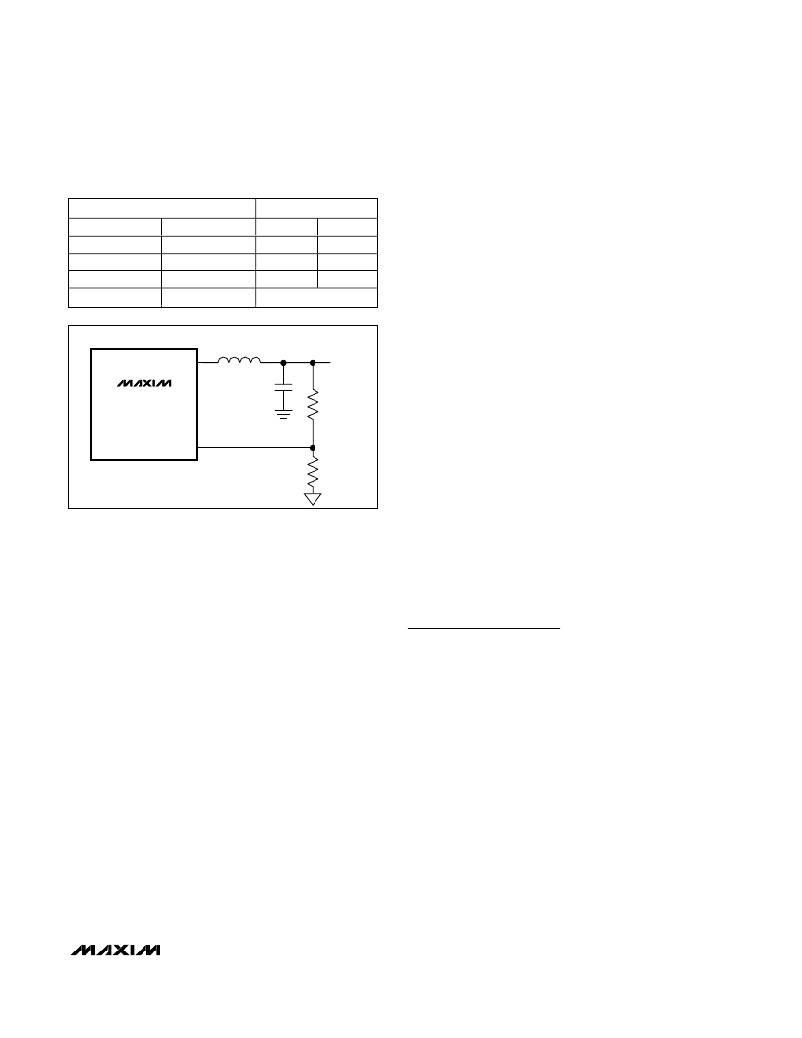
�R1� =� 30k� ?�
�R2� =� R1(V� OUT� /� V� REF� -� 1)�
�LX�
�FB�
�R2�
�R1�
�V� OUT�
�cy� in� PWM� mode.�
�This� number� is� reduced� when� the� switching� frequency�
�decreases� as� the� part� enters� Idle� Mode.� Combined� con-�
�duction� losses� in� the� two� power� switches� are� approxi-�
�mated� by:�
�P� D� =� I� OUT2� x� R� PMOS�
�where� R� PMOS� is� the� on-resistance� of� the� PMOS� switch.�
�The� junction-to-ambient� thermal� resistance� required� to�
�dissipate� this� amount� of� power� is� calculated� by:�
�V� REF� =� 1.1V�
�Figure� 4.� Adjustable� Output� Voltage�
�Synchronous� Rectification�
�In� a� step-down� regulator� without� synchronous� rectifica-�
�tion,� an� external� Schottky� diode� provides� a� path� for� cur-�
�rent� to� flow� when� the� inductor� is� discharging.� Replacing�
�the� Schottky� diode� with� a� low-resistance� NMOS� syn-�
�chronous� switch� reduces� conduction� losses� and�
�improves� efficiency.�
�The� NMOS� synchronous-rectifier� switch� turns� on� follow-�
�ing� a� short� delay� after� the� PMOS� power� switch� turns� off,�
�thus� preventing� cross� conduction� or� “� shoot� through.� ”� In�
�constant-off-time� mode,� the� synchronous-rectifier�
�switch� turns� off� just� prior� to� the� PMOS� power� switch�
�turning� on.� While� both� switches� are� off,� inductor� current�
�flows� through� the� internal-body� diode� of� the� NMOS�
�switch.� The� internal-body� diode� ’� s� forward� voltage� is� rel-�
�atively� high.� An� external� Schottky� diode� from� PGND� to�
�LX� can� improve� efficiency.�
�Thermal� Resistance�
�Junction-to-ambient� thermal� resistance,� θ� JA� ,� is� highly�
�dependent� on� the� amount� of� copper� area� immediately�
�surrounding� the� IC� leads.� The� MAX1830/MAX1831�
�evaluation� kit� has� 0.7in� 2� of� copper� area� and� a� thermal�
�resistance� of� +71� °� C/W� with� no� forced� airflow.� Airflow�
�over� the� board� significantly� reduces� the� junction-to-�
�ambient� thermal� resistance.� For� heatsinking� purposes,�
�θ� JA� =� (T� J,MAX� -� T� A,MAX� )� /� P� D(T� OT� )�
�where:�
�θ� JA� =� junction-to-ambient� thermal� resistance�
�T� J,MAX� =� maximum� junction� temperature�
�T� A,MAX� =� maximum� ambient� temperature�
�P� D(TOT)� =� total� losses�
�Design� Procedure�
�For� typical� applications,� use� the� recommended� compo-�
�nent� values� in� Table� 1.� For� other� applications,� take� the�
�following� steps:�
�1)� Select� the� desired� PWM-mode� switching� frequency;�
�1MHz� is� a� good� starting� point.� See� Figure� 3� for� maxi-�
�mum� operating� frequency.�
�2)� Select� the� constant� off-time� as� a� function� of� input�
�voltage,� output� voltage,� and� switching� frequency.�
�3)� Select� R� TOFF� as� a� function� of� off-time.�
�4)� Select� the� inductor� as� a� function� of� output� voltage,�
�off-time,� and� peak-to-peak� inductor� current.�
�Setting� the� Output� Voltage�
�The� output� of� the� MAX1830/MAX1831� is� selectable�
�between� one� of� three� preset� output� voltages.� For� a� pre-�
�set� output� voltage,� connect� FB� to� the� output� voltage�
�and� connect� FBSEL� as� indicated� in� Table� 2.� For� an�
�adjustable� output� voltage,� connect� FBSEL� to� GND� and�
�connect� FB� to� a� resistive� divider� between� the� output�
�_______________________________________________________________________________________�
�9�
�相关PDF资料 |
PDF描述 |
|---|---|
| MAX1835EUT#TG16 | IC REG BOOST SYNC 3.3V SOT23-6 |
| MAX1836EUT33#TG16 | IC REG BUCK 3.3V 125MA SOT23-6 |
| MAX1838EEE+ | IC SW USB DUAL W/FB 16-QSOP |
| MAX1842EEE+T | IC REG BUCK SYNC 1A 16QSOP |
| MAX1843ETI+ | IC REG BUCK SYNC 2.7A 28TQFN |
相关代理商/技术参数 |
参数描述 |
|---|---|
| MAX1830EVKIT | 功能描述:电源管理IC开发工具 RoHS:否 制造商:Maxim Integrated 产品:Evaluation Kits 类型:Battery Management 工具用于评估:MAX17710GB 输入电压: 输出电压:1.8 V |
| MAX1830EVKIT+ | 功能描述:电源管理IC开发工具 Evaluation Kit for the MAX1830 RoHS:否 制造商:Maxim Integrated 产品:Evaluation Kits 类型:Battery Management 工具用于评估:MAX17710GB 输入电压: 输出电压:1.8 V |
| MAX1831EEE | 功能描述:直流/直流开关调节器 RoHS:否 制造商:International Rectifier 最大输入电压:21 V 开关频率:1.5 MHz 输出电压:0.5 V to 0.86 V 输出电流:4 A 输出端数量: 最大工作温度: 安装风格:SMD/SMT 封装 / 箱体:PQFN 4 x 5 |
| MAX1831EEE+ | 功能描述:直流/直流开关调节器 3A 1MHz Step-Down RoHS:否 制造商:International Rectifier 最大输入电压:21 V 开关频率:1.5 MHz 输出电压:0.5 V to 0.86 V 输出电流:4 A 输出端数量: 最大工作温度: 安装风格:SMD/SMT 封装 / 箱体:PQFN 4 x 5 |
| MAX1831EEE+T | 功能描述:直流/直流开关调节器 3A 1MHz Step-Down RoHS:否 制造商:International Rectifier 最大输入电压:21 V 开关频率:1.5 MHz 输出电压:0.5 V to 0.86 V 输出电流:4 A 输出端数量: 最大工作温度: 安装风格:SMD/SMT 封装 / 箱体:PQFN 4 x 5 |
发布紧急采购,3分钟左右您将得到回复。