- 您现在的位置:买卖IC网 > PDF目录383338 > MAX1858A (Maxim Integrated Products, Inc.) Dual 180?Out-of-Phase Buck Controllers with Sequencing/Prebias Startup and POR PDF资料下载
参数资料
| 型号: | MAX1858A |
| 厂商: | Maxim Integrated Products, Inc. |
| 英文描述: | Dual 180?Out-of-Phase Buck Controllers with Sequencing/Prebias Startup and POR |
| 中文描述: | 双路、180°异相工作的buck控制器,具有排序/预偏置启动和POR |
| 文件页数: | 7/22页 |
| 文件大小: | 553K |
| 代理商: | MAX1858A |
Detailed Description
DC-DC PWM Controller
The MAX1858A/MAX1875A/MAX1876A step-down con-
verters use a PWM voltage-mode control scheme (Figure
2) for each out-of-phase controller. The controller gener-
ates the clock signal by dividing down the internal oscil-
lator or SYNC input when driven by an external clock, so
each controller
’
s switching frequency equals half the
oscillator frequency (f
SW
= f
OSC
/2). An internal transcon-
ductance error amplifier produces an integrated error
voltage at the COMP pin, providing high DC accuracy.
The voltage at COMP sets the duty cycle using a PWM
comparator and a ramp generator. At each rising edge
of the clock, REG1
’
s high-side N-channel MOSFET turns
on and remains on until either the appropriate duty cycle
or until the maximum duty cycle is reached. REG2 oper-
ates out-of-phase, so the second high-side MOSFET
turns on at each falling edge of the clock. During each
high-side MOSFET
’
s on-time, the associated inductor
current ramps up.
During the second-half of the switching cycle, the high-
side MOSFET turns off and the low-side N-channel
MOSFET turns on. Now the inductor releases the stored
energy as its current ramps down, providing current to
the output. Under overload conditions, when the induc-
tor current exceeds the selected valley current limit (see
the
Current-Limit Circuit (ILIM_)
section), the high-side
MOSFET does not turn on at the appropriate clock edge
and the low-side MOSFET remains on to let the inductor
current ramp down.
Synchronized Out-of-Phase Operation
The two independent regulators in the MAX1858A/
MAX1875A/MAX1876A operate 180
°
out-of-phase to
reduce input filtering requirements, reduce electromag-
netic interference (EMI), and improve efficiency. This
effectively lowers component cost and saves board
space, making the MAX1858A/MAX1875A/MAX1876A
ideal for cost-sensitive applications.
Dual-switching regulators typically operate both
controllers in-phase, and turn on both high-side
MOSFETs at the same time. The input capacitor must
then support the instantaneous current requirements of
both controllers simultaneously, resulting in increased
ripple voltage and current when compared to a single
switching regulator. The higher RMS ripple current
lowers efficiency due to power loss associated with the
input capacitor
’
s effective series resistance (ESR). This
typically requires more low-ESR input capacitors in
parallel to minimize input voltage ripple and ESR-related
losses, or to meet the necessary ripple-current rating.
M
Dual 180° Out-of-Phase Buck Controllers with
Sequencing/Prebias Startup and POR
_______________________________________________________________________________________
7
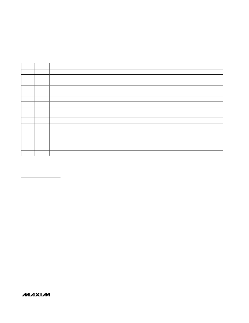
Pin Description (continued)
PIN
14
NAME
DH1
FUNCTION
High-Side Gate-Driver Output for Regulator 1 (REG1). DH1 swings from LX1 to BST1. DH1 is low
during UVLO.
15
LX1
External Inductor Connection for Regulator 1 (REG1). Connect LX1 to the switched side of the inductor. LX1
serves as the lower supply rail for the DH1 high-side gate driver.
16
BST1
Boost Flying-Capacitor Connection for Regulator 1 (REG1). Connect BST1 to an external ceramic capacitor and
diode according to Figure 1.
Low-Side Gate-Driver Output for Regulator 1 (REG1). DL1 swings from PGND to V
L
. DL1 is low
during UVLO.
Power Ground
17
18
DL1
PGND
19
V
L
Internal 5V Linear-Regulator Output. Supplies the regulators and powers the low-side gate drivers and external
boost circuitry for the high-side gate drivers.
Low-Side Gate-Driver Output for Regulator 2 (REG2). DL2 swings from PGND to V
L
. DL2 is low
during UVLO.
Boost Flying-Capacitor Connection for Regulator 2 (REG2). Connect BST2 to an external ceramic capacitor and
diode according to Figure 1.
20
DL2
21
BST2
22
LX2
External Inductor Connection for Regulator 2 (REG2). Connect LX2 to the switched side of the inductor. LX2
serves as the lower supply rail for the DH2 high-side gate driver.
High-Side Gate-Driver Output for Regulator 2 (REG2). DH2 swings from LX2 to BST2. DH2 is low
during UVLO.
Active-High Enable Input. A logic low shuts down both controllers. Connect to V
L
for always-on operation.
23
24
DH2
EN
相关PDF资料 |
PDF描述 |
|---|---|
| MAX1875A | Dual 180?Out-of-Phase Buck Controllers with Sequencing/Prebias Startup and POR |
| MAX1876A | Dual 180?Out-of-Phase Buck Controllers with Sequencing/Prebias Startup and POR |
| MAX1858AEEG | Dual 180∑ Out-of-Phase Buck Controllers with Sequencing/Prebias Startup and POR |
| MAX186CMJP | Low-Power, 8-Channel, Serial 12-Bit ADCs |
| MAX186ACAP | Low-Power, 8-Channel, Serial 12-Bit ADCs |
相关代理商/技术参数 |
参数描述 |
|---|---|
| MAX1858AEEG | 功能描述:DC/DC 开关控制器 RoHS:否 制造商:Texas Instruments 输入电压:6 V to 100 V 开关频率: 输出电压:1.215 V to 80 V 输出电流:3.5 A 输出端数量:1 最大工作温度:+ 125 C 安装风格: 封装 / 箱体:CPAK |
| MAX1858AEEG+ | 功能描述:电压模式 PWM 控制器 Dual 180 Out Buck Controllers RoHS:否 制造商:Texas Instruments 输出端数量:1 拓扑结构:Buck 输出电压:34 V 输出电流: 开关频率: 工作电源电压:4.5 V to 5.5 V 电源电流:600 uA 最大工作温度:+ 125 C 最小工作温度:- 40 C 封装 / 箱体:WSON-8 封装:Reel |
| MAX1858AEEG+T | 功能描述:电压模式 PWM 控制器 Dual 180 Out Buck Controllers RoHS:否 制造商:Texas Instruments 输出端数量:1 拓扑结构:Buck 输出电压:34 V 输出电流: 开关频率: 工作电源电压:4.5 V to 5.5 V 电源电流:600 uA 最大工作温度:+ 125 C 最小工作温度:- 40 C 封装 / 箱体:WSON-8 封装:Reel |
| MAX1858AEEG-T | 功能描述:DC/DC 开关控制器 RoHS:否 制造商:Texas Instruments 输入电压:6 V to 100 V 开关频率: 输出电压:1.215 V to 80 V 输出电流:3.5 A 输出端数量:1 最大工作温度:+ 125 C 安装风格: 封装 / 箱体:CPAK |
| MAX1858EEG | 功能描述:DC/DC 开关控制器 RoHS:否 制造商:Texas Instruments 输入电压:6 V to 100 V 开关频率: 输出电压:1.215 V to 80 V 输出电流:3.5 A 输出端数量:1 最大工作温度:+ 125 C 安装风格: 封装 / 箱体:CPAK |
发布紧急采购,3分钟左右您将得到回复。