- 您现在的位置:买卖IC网 > PDF目录383338 > MAX1858AEEG (MAXIM INTEGRATED PRODUCTS INC) Dual 180∑ Out-of-Phase Buck Controllers with Sequencing/Prebias Startup and POR PDF资料下载
参数资料
| 型号: | MAX1858AEEG |
| 厂商: | MAXIM INTEGRATED PRODUCTS INC |
| 元件分类: | 稳压器 |
| 英文描述: | Dual 180∑ Out-of-Phase Buck Controllers with Sequencing/Prebias Startup and POR |
| 中文描述: | DUAL SWITCHING CONTROLLER, 660 kHz SWITCHING FREQ-MAX, PDSO24 |
| 封装: | 0.150 INCH, 0.25 INCH PITCH, MO-137AE, QSOP-24 |
| 文件页数: | 12/22页 |
| 文件大小: | 553K |
| 代理商: | MAX1858AEEG |
M
Dual 180° Out-of-Phase Buck Controllers with
Sequencing/Prebias Startup and POR
12
______________________________________________________________________________________
High-Side Gate-Drive Supply (BST_)
Gate-drive voltages for the high-side N-channel switch-
es are generated by the flying-capacitor boost circuits
(Figure 5). A boost capacitor (connected from BST_ to
LX_) provides power to the high-side MOSFET driver.
On startup, the synchronous rectifier (low-side MOSFET)
forces LX_ to ground and charges the boost capacitor to
5V. On the second half-cycle, after the low-side MOSFET
turns off, the high-side MOSFET is turned on by closing
an internal switch between BST_ and DH_. This provides
the necessary gate-to-source voltage to turn on the high-
side switch, an action that boosts the 5V gate-drive
signal above V
IN
. The current required to drive the high-
side MOSFET gates (f
SWITCH
Q
G
) is ultimately drawn
from V
L
.
MOSFET Gate Drivers (DH_, DL_)
The DH and DL drivers are optimized for driving moder-
ate-size N-channel high-side and larger low-side power
MOSFETs. This is consistent with the low duty factor
seen with large V
IN
- V
OUT
differential. The DL_ low-side
drive waveform is always the complement of the DH_
high-side drive waveform (with controlled dead time to
prevent cross-conduction or
“
shoot-through
”
). An adap-
tive dead-time circuit monitors the DL_ output and pre-
vents the high-side FET from turning on until DL_ is fully
off. There must be a low-resistance, low-inductance path
from the DL_ driver to the MOSFET gate in order for the
adaptive dead-time circuit to work properly. Otherwise,
the sense circuitry in the MAX1858A/MAX1875A/
MAX1876A interprets the MOSFET gate as
“
off
”
while
there is actually charge still left on the gate. Use very
short, wide traces (50mils to 100mils wide if the MOSFET
is 1in from the device). The dead time at the DH-off edge
is determined by a fixed 30ns internal delay.
Synchronous rectification reduces conduction losses in
the rectifier by replacing the normal low-side Schottky
catch diode with a low-resistance MOSFET switch.
Additionally, the MAX1858A/MAX1875A/MAX1876A use
the synchronous rectifier to ensure proper startup of the
boost gate-driver circuit and to provide the current-limit
signal.
The internal pulldown transistor that drives DL_ low is
robust, with a 0.5
(typ) on-resistance. This low on-
resistance helps prevent DL_ from being pulled up dur-
ing the fast rise time of the LX_ node, due to capacitive
coupling from the drain to the gate of the low-side syn-
chronous-rectifier MOSFET. However, for high-current
applications, some combinations of high- and low-side
FETs can cause excessive gate-drain coupling, leading
to poor efficiency, EMI, and shoot-through currents.
This can be remedied by adding a resistor (typically
less than 5
) in series with BST_, which increases the
turn-on time of the high-side FET without degrading the
turn-off time (Figure 5).
Current-Limit Circuit (ILIM_)
The current-limit circuit employs a
“
valley
”
current-sens-
ing algorithm that uses the on-resistance of the low-side
MOSFET as a current-sensing element. If the current-
sense signal is above the current-limit threshold, the
MAX1858A/MAX1875A/MAX1876A do not initiate a new
cycle (Figure 6). Since valley current sensing is
employed, the actual peak current is greater than the
current-limit threshold by an amount equal to the induc-
tor ripple current. Therefore, the exact current-limit char-
acteristic and maximum load capability are a function of
the low-side MOSFET
’
s on-resistance, current-limit
threshold, inductor value, and input voltage. The reward
for this uncertainty is robust, lossless overcurrent sens-
ing that does not require costly sense resistors.
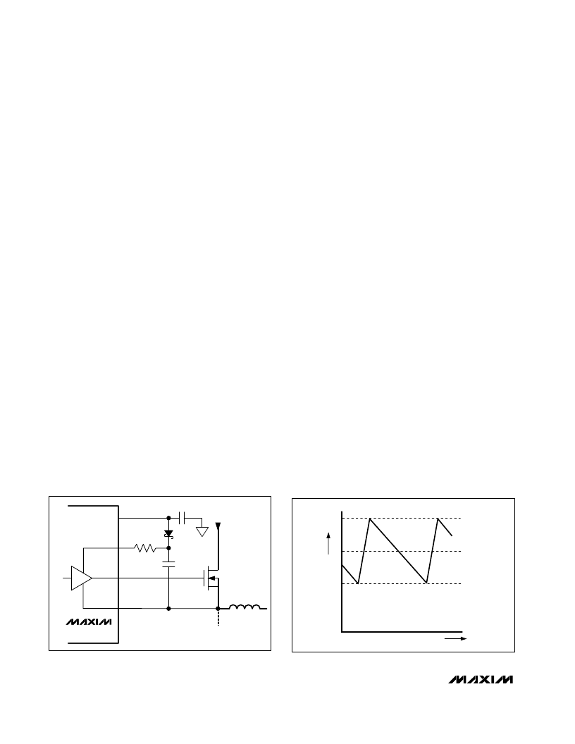
V
L
BST_
DH_
LX_
4.7
INPUT
(V
IN
)
MAX1875A
Figure 5. Reducing the Switching-Node Rise Time
I
I
LIMIT
I
LOAD
0
TIME
-I
PEAK
Figure 6.
“
Valley
”
Current-Limit Threshold Point
相关PDF资料 |
PDF描述 |
|---|---|
| MAX186CMJP | Low-Power, 8-Channel, Serial 12-Bit ADCs |
| MAX186ACAP | Low-Power, 8-Channel, Serial 12-Bit ADCs |
| MAX186ACPP | Low-Power, 8-Channel, Serial 12-Bit ADCs |
| MAX186ACWP | Low-Power, 8-Channel, Serial 12-Bit ADCs |
| MAX186CCAP | Low-Power, 8-Channel, Serial 12-Bit ADCs |
相关代理商/技术参数 |
参数描述 |
|---|---|
| MAX1858AEEG+ | 功能描述:电压模式 PWM 控制器 Dual 180 Out Buck Controllers RoHS:否 制造商:Texas Instruments 输出端数量:1 拓扑结构:Buck 输出电压:34 V 输出电流: 开关频率: 工作电源电压:4.5 V to 5.5 V 电源电流:600 uA 最大工作温度:+ 125 C 最小工作温度:- 40 C 封装 / 箱体:WSON-8 封装:Reel |
| MAX1858AEEG+T | 功能描述:电压模式 PWM 控制器 Dual 180 Out Buck Controllers RoHS:否 制造商:Texas Instruments 输出端数量:1 拓扑结构:Buck 输出电压:34 V 输出电流: 开关频率: 工作电源电压:4.5 V to 5.5 V 电源电流:600 uA 最大工作温度:+ 125 C 最小工作温度:- 40 C 封装 / 箱体:WSON-8 封装:Reel |
| MAX1858AEEG-T | 功能描述:DC/DC 开关控制器 RoHS:否 制造商:Texas Instruments 输入电压:6 V to 100 V 开关频率: 输出电压:1.215 V to 80 V 输出电流:3.5 A 输出端数量:1 最大工作温度:+ 125 C 安装风格: 封装 / 箱体:CPAK |
| MAX1858EEG | 功能描述:DC/DC 开关控制器 RoHS:否 制造商:Texas Instruments 输入电压:6 V to 100 V 开关频率: 输出电压:1.215 V to 80 V 输出电流:3.5 A 输出端数量:1 最大工作温度:+ 125 C 安装风格: 封装 / 箱体:CPAK |
| MAX1858EEG+ | 功能描述:电压模式 PWM 控制器 Dual 180 Out Buck Controllers RoHS:否 制造商:Texas Instruments 输出端数量:1 拓扑结构:Buck 输出电压:34 V 输出电流: 开关频率: 工作电源电压:4.5 V to 5.5 V 电源电流:600 uA 最大工作温度:+ 125 C 最小工作温度:- 40 C 封装 / 箱体:WSON-8 封装:Reel |
发布紧急采购,3分钟左右您将得到回复。