- 您现在的位置:买卖IC网 > PDF目录15488 > MAX1876AEEG+ (Maxim Integrated Products)IC REG CTRLR BUCK PWM VM 24-QSOP PDF资料下载
参数资料
| 型号: | MAX1876AEEG+ |
| 厂商: | Maxim Integrated Products |
| 文件页数: | 15/22页 |
| 文件大小: | 0K |
| 描述: | IC REG CTRLR BUCK PWM VM 24-QSOP |
| 产品培训模块: | Lead (SnPb) Finish for COTS Obsolescence Mitigation Program |
| 标准包装: | 50 |
| PWM 型: | 电压模式 |
| 输出数: | 2 |
| 频率 - 最大: | 660kHz |
| 电源电压: | 4.5 V ~ 23 V |
| 降压: | 是 |
| 升压: | 无 |
| 回扫: | 无 |
| 反相: | 无 |
| 倍增器: | 无 |
| 除法器: | 无 |
| Cuk: | 无 |
| 隔离: | 无 |
| 工作温度: | -40°C ~ 85°C |
| 封装/外壳: | 24-SSOP(0.154",3.90mm 宽) |
| 包装: | 管件 |
�� �
�
�Dual� 180°� Out-of-Phase� Buck� Controllers� with�
�Sequencing/Prebias� Startup� and� POR�
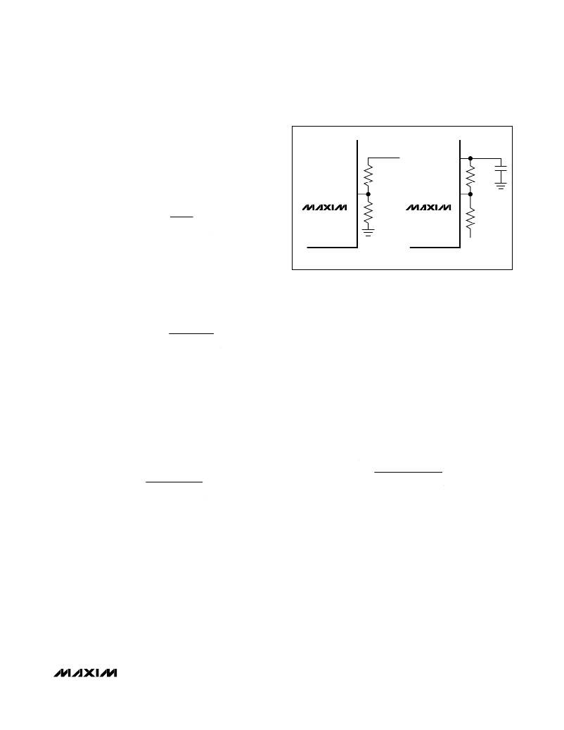
�Setting� the� Output� Voltage�
�For� 1V� or� greater� output� voltages,� set� the� MAX1858A/�
�MAX1875A/MAX1876A� output� voltage� by� connecting� a�
�voltage-divider� from� the� output� to� FB_� to� GND� (Figure�
�8).� Select� R_B� (FB_� to� GND� resistor)� to� between� 1k� ?�
�and� 10k� ?� .� Calculate� R_A� (OUT_� to� FB_� resistor)� with�
�the� following� equation:�
�FB_�
�OUT_�
�R_A�
�REF�
�FB_�
�R_C�
�R� _� A� =� R� _� B� ?� ?� OUT� ?� -1� ?�
�?� ?�
�?� ?� V� ?� ?�
�?� ?� V� SET� ?� ?�
�where� V� SET� =� 1V� (see� the� Electrical� Characteristics� )�
�and� V� OUT� can� range� from� V� SET� to� 18V.�
�For� output� voltages� below� 1V,� set� the� MAX1858A/�
�MAX1858A�
�MAX1875A�
�MAX1876A�
�V� OUT_� >� 1V�
�R_B�
�MAX1858A�
�MAX1875A�
�MAX1876A�
�V� OUT_� <� 1V�
�R_A�
�OUT_�
�R� _� A� =� R� _� C� ?� SET� -� OUT� ?�
�MAX1875A/MAX1876A� output� voltage� by� connecting� a�
�voltage-divider� from� the� output� to� FB_� to� REF� (Figure�
�8).� Select� R_C� (FB� to� REF� resistor)� in� the� 1k� ?� to� 10k� ?�
�range.� Calculate� R_A� with� the� following� equation:�
�?� V V� ?�
�?� V� REF� -� V� SET� ?�
�where� V� SET� =� 1V,� V� REF� =� 2V� (see� the� Electrical�
�Characteristics� ),� and� V� OUT� can� range� from� 0� to� V� SET� .�
�Setting� the� Switching� Frequency�
�The� controller� generates� the� clock� signal� by� dividing�
�down� the� internal� oscillator� or� SYNC� input� signal� when�
�driven� by� an� external� oscillator,� so� the� switching� frequen-�
�cy� equals� half� the� oscillator� frequency� (f� SW� =� f� OSC� /2).�
�The� internal� oscillator� frequency� is� set� by� a� resistor�
�(R� OSC� )� connected� from� OSC� to� GND.� The� relationship�
�between� f� SW� and� R� OSC� is:�
�Figure� 8.� Adjustable� Output� Voltage�
�Inductor� Selection�
�Three� key� inductor� parameters� must� be� specified� for�
�operation� with� the� MAX1858A/MAX1875A/MAX1876A:�
�inductance� value� (L),� peak-inductor� current� (I� PEAK� ),� and�
�DC� resistance� (R� DC� ).� The� following� equation� assumes� a�
�constant� ratio� of� inductor� peak-to-peak� AC� current� to� DC�
�average� current� (LIR).� For� LIR� values� too� high,� the� RMS�
�currents� are� high,� and� therefore� I� 2� R� losses� are� high.�
�Large� inductances� must� be� used� to� achieve� very� low� LIR�
�values.� Typically,� inductance� is� proportional� to� resis-�
�tance� (for� a� given� package� type),� which� again� makes� I� 2� R�
�losses� high� for� very� low� LIR� values.� A� good� compromise�
�between� size� and� loss� is� a� 30%� peak-to-peak� ripple� cur-�
�rent� to� average-current� ratio� (LIR� =� 0.3).� The� switching�
�frequency,� input� voltage,� output� voltage,� and� selected�
�LIR� determine� the� inductor� value� as� follows:�
�L� =� OUT� IN� OUT�
�R� OSC� =�
�6� � 10� 9� (� ?� - Hz)�
�f� SW�
�V (V - V )�
�V� IN� f� SW� I� OUT� LIR�
�where� V� IN� ,� V� OUT� ,� and� I� OUT� are� typical� values� (so� that�
�where� f� SW� is� in� Hz� and� R� OSC� is� in� ?� .� For� example,� a�
�600kHz� switching� frequency� is� set� with� R� OSC� =� 10k� ?� .�
�Higher� frequencies� allow� designs� with� lower� inductor�
�values� and� less� output� capacitance.� Consequently,�
�peak� currents� and� I� 2� R� losses� are� lower� at� higher�
�switching� frequencies,� but� core� losses,� gate-charge�
�currents,� and� switching� losses� increase.�
�A� rising� clock� edge� on� SYNC� is� interpreted� as� a� syn-�
�chronization� input.� If� the� SYNC� signal� is� lost,� the� inter-�
�nal� oscillator� takes� control� of� the� switching� rate,�
�returning� the� switching� frequency� to� that� set� by� R� OSC� .�
�This� maintains� output� regulation� even� with� intermittent�
�SYNC� signals.� When� an� external� synchronization� signal�
�is� used,� R� OSC� should� set� the� switching� frequency� to�
�one-half� SYNC� rate� (f� SYNC� ).�
�efficiency� is� optimum� for� typical� conditions).� The� switch-�
�ing� frequency� is� set� by� R� OSC� (see� the� Setting� the�
�Switching� Frequency� section).� The� exact� inductor� value�
�is� not� critical� and� can� be� adjusted� in� order� to� make�
�trade-offs� among� size,� cost,� and� efficiency.� Lower�
�inductor� values� minimize� size� and� cost,� but� also�
�improve� transient� response� and� reduce� efficiency� due�
�to� higher� peak� currents.� On� the� other� hand,� higher�
�inductance� increases� efficiency� by� reducing� the� RMS�
�current.� However,� resistive� losses� due� to� extra� wire� turns�
�can� exceed� the� benefit� gained� from� lower� AC� current�
�levels,� especially� when� the� inductance� is� increased�
�without� also� allowing� larger� inductor� dimensions.�
�Find� a� low-loss� inductor� having� the� lowest� possible� DC�
�resistance� that� fits� in� the� allotted� dimensions.� The�
�______________________________________________________________________________________�
�15�
�相关PDF资料 |
PDF描述 |
|---|---|
| GCC20DRTN-S93 | CONN EDGECARD 40POS DIP .100 SLD |
| MAX1771EPA+ | IC REG CTRLR BST PWM 8-DIP |
| GCC20DRTH-S93 | CONN EDGECARD 40POS DIP .100 SLD |
| ECC20DRTS-S93 | CONN EDGECARD 40POS DIP .100 SLD |
| MAX1847EEE+ | IC REG CTRLR FLYBK INV CM 16QSOP |
相关代理商/技术参数 |
参数描述 |
|---|---|
| MAX1876AEEG+ | 功能描述:电压模式 PWM 控制器 Dual 180 Out PWM Step-Down RoHS:否 制造商:Texas Instruments 输出端数量:1 拓扑结构:Buck 输出电压:34 V 输出电流: 开关频率: 工作电源电压:4.5 V to 5.5 V 电源电流:600 uA 最大工作温度:+ 125 C 最小工作温度:- 40 C 封装 / 箱体:WSON-8 封装:Reel |
| MAX1876AEEG+T | 功能描述:电压模式 PWM 控制器 Dual 180 Out PWM Step-Down RoHS:否 制造商:Texas Instruments 输出端数量:1 拓扑结构:Buck 输出电压:34 V 输出电流: 开关频率: 工作电源电压:4.5 V to 5.5 V 电源电流:600 uA 最大工作温度:+ 125 C 最小工作温度:- 40 C 封装 / 箱体:WSON-8 封装:Reel |
| MAX1876AEEG-T | 功能描述:DC/DC 开关控制器 RoHS:否 制造商:Texas Instruments 输入电压:6 V to 100 V 开关频率: 输出电压:1.215 V to 80 V 输出电流:3.5 A 输出端数量:1 最大工作温度:+ 125 C 安装风格: 封装 / 箱体:CPAK |
| MAX1876EEG | 功能描述:DC/DC 开关控制器 RoHS:否 制造商:Texas Instruments 输入电压:6 V to 100 V 开关频率: 输出电压:1.215 V to 80 V 输出电流:3.5 A 输出端数量:1 最大工作温度:+ 125 C 安装风格: 封装 / 箱体:CPAK |
| MAX1876EEG+ | 功能描述:电压模式 PWM 控制器 Dual 180 Out PWM Step-Down RoHS:否 制造商:Texas Instruments 输出端数量:1 拓扑结构:Buck 输出电压:34 V 输出电流: 开关频率: 工作电源电压:4.5 V to 5.5 V 电源电流:600 uA 最大工作温度:+ 125 C 最小工作温度:- 40 C 封装 / 箱体:WSON-8 封装:Reel |
发布紧急采购,3分钟左右您将得到回复。