- 您现在的位置:买卖IC网 > PDF目录10558 > MAX187BCWE+ (Maxim Integrated Products)IC ADC SRL12BIT 5V 75KSPS 16SOIC PDF资料下载
参数资料
| 型号: | MAX187BCWE+ |
| 厂商: | Maxim Integrated Products |
| 文件页数: | 2/18页 |
| 文件大小: | 0K |
| 描述: | IC ADC SRL12BIT 5V 75KSPS 16SOIC |
| 产品培训模块: | Lead (SnPb) Finish for COTS Obsolescence Mitigation Program |
| 标准包装: | 46 |
| 位数: | 12 |
| 采样率(每秒): | 75k |
| 数据接口: | MICROWIRE?,QSPI?,串行,SPI? |
| 转换器数目: | 1 |
| 功率耗散(最大): | 478mW |
| 电压电源: | 单电源 |
| 工作温度: | 0°C ~ 70°C |
| 安装类型: | 表面贴装 |
| 封装/外壳: | 16-SOIC(0.295",7.50mm 宽) |
| 供应商设备封装: | 16-SOIC W |
| 包装: | 管件 |
| 输入数目和类型: | 1 个单端,单极 |
| 产品目录页面: | 1393 (CN2011-ZH PDF) |
MAX187/MAX189
+5V, Low-Power, 12-Bit Serial ADCs
10
Maxim Integrated
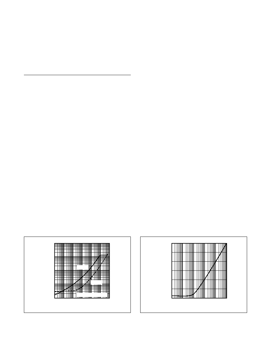
Figure 6. Average Supply Current vs. Conversion Rate
Figure 7. tWAkE vs. Time in Shutdown (MAX187 Only)
Serial Interface
Initialization After Power-Up and
Starting a Conversion
When power is first applied, it takes the fully discharged
4.7FF reference bypass capacitor up to 20ms to provide
adequate charge for specified accuracy. With SHDN
not pulled low, the MAX187/MAX189 are now ready to
convert.
To start a conversion, pull CS low. At CS’s falling edge,
the T/H enters its hold mode and a conversion is initiated.
After an internally timed 8.5Fs conversion period, the end
of conversion is signaled by DOUT pulling high. Data can
then be shifted out serially with the external clock.
Using SHDN to Reduce
Supply Current
Power consumption can be reduced significantly by
shutting down the MAX187/MAX189 between conver-
sions. This is shown in Figure 6, a plot of average supply
current vs. conversion rate. Because the MAX189 uses
an external reference voltage (assumed to be present
continuously), it “wakes up” from shutdown more quickly,
and therefore provides lower average supply currents.
The wakeup-time, tWAKE, is the time from SHDN deas-
serted to the time when a conversion may be initiated.
For the MAX187, this time is 2Fs. For the MAX189, this
time depends on the time in shutdown (see Figure 7)
because the external 4.7FF reference bypass capacitor
loses charge slowly during shutdown (see the specifica-
tions for shutdown, REF Input Current = 10FA max).
External Clock
The actual conversion does not require the external
clock. This frees the FP from the burden of running the
SAR conversion clock, and allows the conversion result
to be read back at the FP’s convenience at any clock rate
from 0 to 5MHz. The clock duty cycle is unrestricted if
each clock phase is at least 100ns. Do not run the clock
while a conversion is in progress.
Timing and Control
Conversion-start and data-read operations are controlled
by the CS and SCLK digital inputs. The timing diagrams
of Figures 8 and 9 outline the operation of the serial
interface.
A CS falling edge initiates a conversion sequence: The
T/H stage holds input voltage, the ADC begins to convert,
and DOUT changes from high impedance to logic low.
SCLK must be kept inactive during the conversion. An
internal register stores the data when the conversion is
in progress.
End of conversion (EOC) is signaled by DOUT going
high. DOUT’s rising edge can be used as a framing sig-
nal. SCLK shifts the data out of this register any time after
the conversion is complete. DOUT transitions on SCLK’s
falling edge. The next falling clock edge produces the
MSB of the conversion at DOUT, followed by the remain-
ing bits. Since there are 12 data bits and one leading
high bit, at least 13 falling clock edges are needed to
shift out these bits. Extra clock pulses occurring after the
conversion result has been clocked out, and prior to a
rising edge of CS, produce trailing 0s at DOUT and have
no effect on converter operation.
CONVERSIONS PER SECOND
SUPPLY
CURRENT
(A)
10k
1k
100
10
1
10
100
1000
10,000
1
0.1
100k
MAX187
MAX189*
*REF CONNECTED TO VDD
TIME IN SHUTDOWN (s)
t WAKE
(ms)
1
0.1
0.01
0.001
0.5
1.0
1.5
2.0
2.5
3.0
0
0.0001
10
相关PDF资料 |
PDF描述 |
|---|---|
| 1445823-3 | CONN RECEPT 11-6POS PANEL MOUNT |
| 1445816-1 | CONN RECEPT 11-9POS PANEL MOUNT |
| MAX187BCPA+ | IC ADC SRL 12BIT 5V 75KSPS 8-DIP |
| VE-B51-IV-F4 | CONVERTER MOD DC/DC 12V 150W |
| VE-B51-IV-F3 | CONVERTER MOD DC/DC 12V 150W |
相关代理商/技术参数 |
参数描述 |
|---|---|
| MAX187BCWE+ | 功能描述:模数转换器 - ADC 12-Bit 75ksps 5.25V Precision ADC RoHS:否 制造商:Texas Instruments 通道数量:2 结构:Sigma-Delta 转换速率:125 SPs to 8 KSPs 分辨率:24 bit 输入类型:Differential 信噪比:107 dB 接口类型:SPI 工作电源电压:1.7 V to 3.6 V, 2.7 V to 5.25 V 最大工作温度:+ 85 C 安装风格:SMD/SMT 封装 / 箱体:VQFN-32 |
| MAX187BCWE+T | 功能描述:模数转换器 - ADC 12-Bit 75ksps 5.25V Precision ADC RoHS:否 制造商:Texas Instruments 通道数量:2 结构:Sigma-Delta 转换速率:125 SPs to 8 KSPs 分辨率:24 bit 输入类型:Differential 信噪比:107 dB 接口类型:SPI 工作电源电压:1.7 V to 3.6 V, 2.7 V to 5.25 V 最大工作温度:+ 85 C 安装风格:SMD/SMT 封装 / 箱体:VQFN-32 |
| MAX187BCWE-T | 功能描述:模数转换器 - ADC RoHS:否 制造商:Texas Instruments 通道数量:2 结构:Sigma-Delta 转换速率:125 SPs to 8 KSPs 分辨率:24 bit 输入类型:Differential 信噪比:107 dB 接口类型:SPI 工作电源电压:1.7 V to 3.6 V, 2.7 V to 5.25 V 最大工作温度:+ 85 C 安装风格:SMD/SMT 封装 / 箱体:VQFN-32 |
| MAX187BEPA | 功能描述:模数转换器 - ADC Integrated Circuits (ICs) RoHS:否 制造商:Texas Instruments 通道数量:2 结构:Sigma-Delta 转换速率:125 SPs to 8 KSPs 分辨率:24 bit 输入类型:Differential 信噪比:107 dB 接口类型:SPI 工作电源电压:1.7 V to 3.6 V, 2.7 V to 5.25 V 最大工作温度:+ 85 C 安装风格:SMD/SMT 封装 / 箱体:VQFN-32 |
| MAX187BEPA+ | 功能描述:模数转换器 - ADC 12-Bit 75ksps 5.25V Precision ADC RoHS:否 制造商:Texas Instruments 通道数量:2 结构:Sigma-Delta 转换速率:125 SPs to 8 KSPs 分辨率:24 bit 输入类型:Differential 信噪比:107 dB 接口类型:SPI 工作电源电压:1.7 V to 3.6 V, 2.7 V to 5.25 V 最大工作温度:+ 85 C 安装风格:SMD/SMT 封装 / 箱体:VQFN-32 |
发布紧急采购,3分钟左右您将得到回复。