- 您现在的位置:买卖IC网 > PDF目录9899 > MAX187BCWE+T (Maxim Integrated Products)IC ADC 12BIT SERIAL LP 16SOIC PDF资料下载
参数资料
| 型号: | MAX187BCWE+T |
| 厂商: | Maxim Integrated Products |
| 文件页数: | 5/18页 |
| 文件大小: | 0K |
| 描述: | IC ADC 12BIT SERIAL LP 16SOIC |
| 产品培训模块: | Lead (SnPb) Finish for COTS Obsolescence Mitigation Program |
| 标准包装: | 1,000 |
| 位数: | 12 |
| 采样率(每秒): | 75k |
| 数据接口: | MICROWIRE?,QSPI?,串行,SPI? |
| 转换器数目: | 1 |
| 功率耗散(最大): | 478mW |
| 电压电源: | 单电源 |
| 工作温度: | 0°C ~ 70°C |
| 安装类型: | 表面贴装 |
| 封装/外壳: | 16-SOIC(0.295",7.50mm 宽) |
| 供应商设备封装: | 16-SOIC W |
| 包装: | 带卷 (TR) |
| 输入数目和类型: | 1 个单端,单极 |
MAX187/MAX189
+5V, Low-Power, 12-Bit Serial ADCs
13
Maxim Integrated
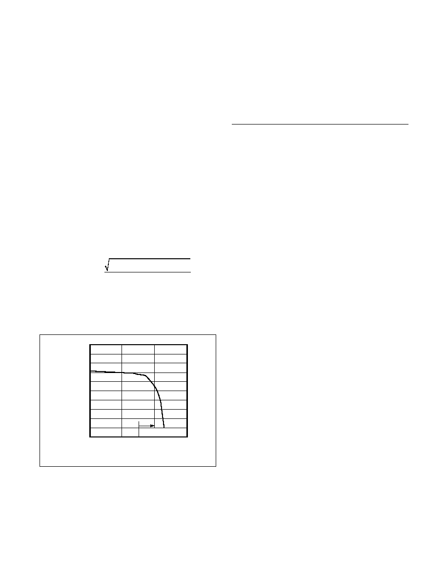
Figure 12. Effective Bits vs. Input Frequency
The effective resolution (effective number of bits) the
ADC provides can be determined by transposing the
above equation and substituting in the measured SINAD:
N = (SINAD - 1.76)/6.02. Figure 12 shows the effective
number of bits as a function of the input frequency for the
MAX187/MAX189.
Total Harmonic Distortion
If a pure sine wave is sampled by an ADC at greater than
the Nyquist frequency, the nonlinearities in the ADC’s
transfer function create harmonics of the input frequency
present in the sampled output data.
Total Harmonic Distortion (THD) is the ratio of the RMS
sum of all the harmonics (in the frequency band above
DC and below one-half the sample rate, but not including
the DC component) to the RMS amplitude of the funda-
mental frequency. This is expressed as follows:
22
2
23
4
N
1
VVV
V
THD 20log
V
+
+…
=
where V1 is the fundamental RMS amplitude, and V2
through VN are the amplitudes of the 2nd through
Nth harmonics. The THD specification in the Electrical
Characteristics includes the 2nd through 5th harmonics.
Applications Information
Connection to Standard Interfaces
The MAX187/MAX189 serial interface is fully compatible
with SPI, QSPI, and MICROWIRE standard serial inter-
faces.
If a serial interface is available, set the CPU’s serial inter-
face in master mode so the CPU generates the serial
clock. Choose a clock frequency up to 2.5MHz.
1) Use a general-purpose I/O line on the CPU to pull CS
low. Keep SCLK low.
2) Wait the for the maximum conversion time specified
before activating SCLK. Alternatively, look for a DOUT
rising edge to determine the end of conversion.
3) Activate SCLK for a minimum of 13 clock cycles.
The first falling clock edge will produce the MSB of
the DOUT conversion. DOUT output data transitions
on SCLK’s falling edge and is available in MSB-first
format. Observe the SCLK to DOUT valid timing char-
acteristic. Data can be clocked into the FP on SCLK’s
rising edge.
4) Pull CS high at or after the 13th falling clock edge. If
CS remains low, trailing zeros are clocked out after
the LSB.
5) With CS = high, wait the minimum specified time, tCS,
before launching a new conversion by pulling CS low.
If a conversion is aborted by pulling CS high before
the conversions end, wait for the minimum acquisition
time, tACQ, before starting a new conversion.
Data can be output in 1-byte chunks or continuously, as
shown in Figure 8. The bytes will contain the result of the
conversion padded with one leading 1, and trailing 0s if
SCLK is still active with CS kept low.
SPI and MICROWIRE
When using SPI or QSPI, set CPOL = 0 and CPHA = 0.
Conversion begins with a CS falling edge. DOUT goes
low, indicating a conversion in progress. Wait until DOUT
goes high or the maximum specified 8.5Fs conversion
time. Two consecutive 1-byte reads are required to get
the full 12 bits from the ADC. DOUT output data transi-
tions on SCLK’s falling edge and is clocked into the FP
on SCLK’s rising edge.
The first byte contains a leading 1 and 7 bits of conver-
sion result. The second byte contains the remaining 5
bits and 3 trailing 0s. See Figure 13 for connections and
Figure 14 for timing.
11.8
11.6
11.4
11.2
11.0
10.8
10.6
10.4
10.2
110
100
1000
EFFECTIVE
BITS
INPUT FREQUENCY (kHz)
12.0
12.2
(UNDERSAMPLED)
相关PDF资料 |
PDF描述 |
|---|---|
| IDT72V2105L10PF8 | IC FIFO SUPERSYNCII 10NS 64-TQFP |
| MAX1499ECJ+T | IC ADC 3 1/2DIG W/LED DVR 32TQFP |
| MS27472E18F28S | CONN RCPT 28POS WALL MT W/SCKT |
| ISL32272EFBZ | IC XMITTER ESD RS422 LP 16-SOIC |
| ISL32179EIRZ | IC XMITTER ESD RS422 LP 24-QFN |
相关代理商/技术参数 |
参数描述 |
|---|---|
| MAX187BEPA | 功能描述:模数转换器 - ADC Integrated Circuits (ICs) RoHS:否 制造商:Texas Instruments 通道数量:2 结构:Sigma-Delta 转换速率:125 SPs to 8 KSPs 分辨率:24 bit 输入类型:Differential 信噪比:107 dB 接口类型:SPI 工作电源电压:1.7 V to 3.6 V, 2.7 V to 5.25 V 最大工作温度:+ 85 C 安装风格:SMD/SMT 封装 / 箱体:VQFN-32 |
| MAX187BEPA+ | 功能描述:模数转换器 - ADC 12-Bit 75ksps 5.25V Precision ADC RoHS:否 制造商:Texas Instruments 通道数量:2 结构:Sigma-Delta 转换速率:125 SPs to 8 KSPs 分辨率:24 bit 输入类型:Differential 信噪比:107 dB 接口类型:SPI 工作电源电压:1.7 V to 3.6 V, 2.7 V to 5.25 V 最大工作温度:+ 85 C 安装风格:SMD/SMT 封装 / 箱体:VQFN-32 |
| MAX187BEWE | 功能描述:模数转换器 - ADC Integrated Circuits (ICs) RoHS:否 制造商:Texas Instruments 通道数量:2 结构:Sigma-Delta 转换速率:125 SPs to 8 KSPs 分辨率:24 bit 输入类型:Differential 信噪比:107 dB 接口类型:SPI 工作电源电压:1.7 V to 3.6 V, 2.7 V to 5.25 V 最大工作温度:+ 85 C 安装风格:SMD/SMT 封装 / 箱体:VQFN-32 |
| MAX187BEWE+ | 功能描述:模数转换器 - ADC 12-Bit 75ksps 5.25V Precision ADC RoHS:否 制造商:Texas Instruments 通道数量:2 结构:Sigma-Delta 转换速率:125 SPs to 8 KSPs 分辨率:24 bit 输入类型:Differential 信噪比:107 dB 接口类型:SPI 工作电源电压:1.7 V to 3.6 V, 2.7 V to 5.25 V 最大工作温度:+ 85 C 安装风格:SMD/SMT 封装 / 箱体:VQFN-32 |
| MAX187BEWE+T | 功能描述:模数转换器 - ADC 12-Bit 75ksps 5.25V Precision ADC RoHS:否 制造商:Texas Instruments 通道数量:2 结构:Sigma-Delta 转换速率:125 SPs to 8 KSPs 分辨率:24 bit 输入类型:Differential 信噪比:107 dB 接口类型:SPI 工作电源电压:1.7 V to 3.6 V, 2.7 V to 5.25 V 最大工作温度:+ 85 C 安装风格:SMD/SMT 封装 / 箱体:VQFN-32 |
发布紧急采购,3分钟左右您将得到回复。