- 您现在的位置:买卖IC网 > PDF目录383340 > MAX187CCWE (MAXIM INTEGRATED PRODUCTS INC) +5V, Low-Power, 12-Bit Serial ADCs PDF资料下载
参数资料
| 型号: | MAX187CCWE |
| 厂商: | MAXIM INTEGRATED PRODUCTS INC |
| 元件分类: | ADC |
| 英文描述: | +5V, Low-Power, 12-Bit Serial ADCs |
| 中文描述: | 1-CH 12-BIT SUCCESSIVE APPROXIMATION ADC, SERIAL ACCESS, PDSO16 |
| 封装: | 0.300 INCH, SOP-16 |
| 文件页数: | 11/20页 |
| 文件大小: | 177K |
| 代理商: | MAX187CCWE |
____________________S erial Interfac e
Initialization After Power-Up and
S tarting a Conversion
When power is first applied, it takes the fully dis-
charged 4.7μF reference bypass capacitor up to 20ms
to provide adequate charge for specified accuracy.
With
SHDN
not pulled low, the MAX187/MAX189 are
now ready to convert.
To start a conversion, pull
CS
low. At
CS
’s
falling edge,
the T/H enters its hold mode and a conversion is initiat-
ed. After an internally timed 8.5μs conversion period,
the end of conversion is signaled by DOUT pulling
high. Data can then be shifted out serially with the
external clock.
Using
SHDN
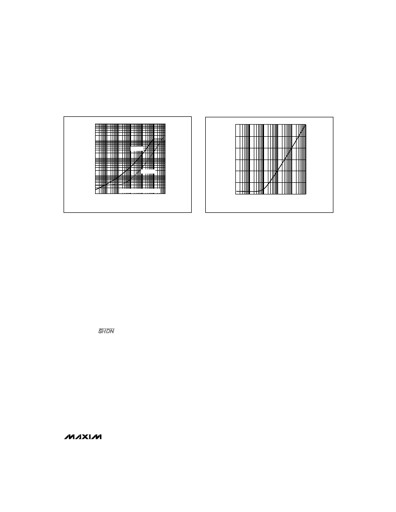
to Reduc e S upply Current
Power consumption can be reduced significantly by
shutting down the MAX187/MAX189 between conver-
sions. This is shown in Figure 6, a plot of average sup-
ply current vs. conversion rate. Because the MAX189
uses an external reference voltage (assumed to be pre-
sent continuously), it "wakes up" from shutdown more
quickly, and therefore provides lower average supply
currents. The wakeup-time, t
WAKE,
is the time from
SHDN
deasserted to the time when a conversion may
be initiated. For the MAX187, this time is 2μs. For the
MAX189, this time depends on the time in shutdown
(see Figure 7) because the external 4.7μF reference
bypass capacitor loses charge slowly during shutdown
(see the specifications for shutdown, REF Input Current
= 10μA max).
External Cloc k
The actual conversion does not require the external
clock. This frees the μP from the burden of running the
SAR conversion clock, and allows the conversion result
to be read back at the μP’s convenience at any clock
rate from 0MHz to 5MHz. The clock duty cycle is unre-
stricted if each clock phase is at least 100ns. Do not
run the clock while a conversion is in progress.
T iming and Control
Conversion-start and data-read operations are con-
trolled by the
CS
and SCLK digital inputs. The timing
diagrams of Figures 8 and 9 outline the operation of the
serial interface.
A
CS
falling edge initiates a conversion sequence: The
T/H stage holds input voltage, the ADC begins to con-
vert, and DOUT changes from high impedance to logic
low. SCLK must be kept inactive during the conversion.
An internal register stores the data when the conversion
is in progress.
End of conversion (EOC) is signaled by DOUT going
high. DOUT’s rising edge can be used as a framing
signal. SCLK shifts the data out of this register any time
after the conversion is complete. DOUT transitions on
SCLK’s falling edge. The next falling clock edge pro-
duces the MSB of the conversion at DOUT, followed by
the remaining bits. Since there are 12 data bits and one
leading high bit, at least 13 falling clock edges are
needed to shift out these bits. Extra clock pulses occur-
ring after the conversion result has been clocked out,
and prior to a rising edge of
CS
, produce trailing 0s at
DOUT and have no effect on converter operation.
+5V, Low-Power, 12-Bit S erial ADCs
______________________________________________________________________________________
11
10000
1000
100
10
1
0.1
1
10
100
1000
10000
CONVERSIONS PER SECOND
S
μ
A
100000
MAX187
MAX189*
*REF CONNECTED TOV
DD
3.0
2.5
2.0
1.5
1.0
0.5
0
0.0001
0.001
0.01
0.1
1
10
TIME IN SHUTDOWN (sec)
t
W
M
Figure 6. Average Supply Current vs. Conversion Rate
Figure 7. t
WAKE
vs. Time in Shutdown (MAX187 only)
相关PDF资料 |
PDF描述 |
|---|---|
| MAX189CCWE | +5V, Low-Power, 12-Bit Serial ADCs |
| MAX189CCPA | +5V, Low-Power, 12-Bit Serial ADCs |
| MAX189BCWE | +5V, Low-Power, 12-Bit Serial ADCs |
| MAX189ACPA | +5V, Low-Power, 12-Bit Serial ADCs |
| MAX189ACWE | +5V, Low-Power, 12-Bit Serial ADCs |
相关代理商/技术参数 |
参数描述 |
|---|---|
| MAX187CCWE+ | 功能描述:模数转换器 - ADC 12-Bit 75ksps 5.25V Precision ADC RoHS:否 制造商:Texas Instruments 通道数量:2 结构:Sigma-Delta 转换速率:125 SPs to 8 KSPs 分辨率:24 bit 输入类型:Differential 信噪比:107 dB 接口类型:SPI 工作电源电压:1.7 V to 3.6 V, 2.7 V to 5.25 V 最大工作温度:+ 85 C 安装风格:SMD/SMT 封装 / 箱体:VQFN-32 |
| MAX187CCWE+T | 功能描述:模数转换器 - ADC 12-Bit 75ksps 5.25V Precision ADC RoHS:否 制造商:Texas Instruments 通道数量:2 结构:Sigma-Delta 转换速率:125 SPs to 8 KSPs 分辨率:24 bit 输入类型:Differential 信噪比:107 dB 接口类型:SPI 工作电源电压:1.7 V to 3.6 V, 2.7 V to 5.25 V 最大工作温度:+ 85 C 安装风格:SMD/SMT 封装 / 箱体:VQFN-32 |
| MAX187CCWE-T | 功能描述:模数转换器 - ADC RoHS:否 制造商:Texas Instruments 通道数量:2 结构:Sigma-Delta 转换速率:125 SPs to 8 KSPs 分辨率:24 bit 输入类型:Differential 信噪比:107 dB 接口类型:SPI 工作电源电压:1.7 V to 3.6 V, 2.7 V to 5.25 V 最大工作温度:+ 85 C 安装风格:SMD/SMT 封装 / 箱体:VQFN-32 |
| MAX187CEPA | 功能描述:模数转换器 - ADC RoHS:否 制造商:Texas Instruments 通道数量:2 结构:Sigma-Delta 转换速率:125 SPs to 8 KSPs 分辨率:24 bit 输入类型:Differential 信噪比:107 dB 接口类型:SPI 工作电源电压:1.7 V to 3.6 V, 2.7 V to 5.25 V 最大工作温度:+ 85 C 安装风格:SMD/SMT 封装 / 箱体:VQFN-32 |
| MAX187CEPA+ | 功能描述:模数转换器 - ADC 12-Bit 75ksps 5.25V Precision ADC RoHS:否 制造商:Texas Instruments 通道数量:2 结构:Sigma-Delta 转换速率:125 SPs to 8 KSPs 分辨率:24 bit 输入类型:Differential 信噪比:107 dB 接口类型:SPI 工作电源电压:1.7 V to 3.6 V, 2.7 V to 5.25 V 最大工作温度:+ 85 C 安装风格:SMD/SMT 封装 / 箱体:VQFN-32 |
发布紧急采购,3分钟左右您将得到回复。