- 您现在的位置:买卖IC网 > PDF目录9457 > MAX188ACAP+ (Maxim Integrated Products)IC ADC 12BIT SERIAL 20-SSOP PDF资料下载
参数资料
| 型号: | MAX188ACAP+ |
| 厂商: | Maxim Integrated Products |
| 文件页数: | 24/25页 |
| 文件大小: | 0K |
| 描述: | IC ADC 12BIT SERIAL 20-SSOP |
| 产品培训模块: | Lead (SnPb) Finish for COTS Obsolescence Mitigation Program |
| 标准包装: | 66 |
| 类型: | 数据采集系统(DAS) |
| 分辨率(位): | 12 b |
| 采样率(每秒): | 133k |
| 数据接口: | MICROWIRE?,QSPI?,串行,SPI? |
| 电压电源: | 双 ± |
| 电源电压: | ±5V |
| 工作温度: | 0°C ~ 70°C |
| 安装类型: | 表面贴装 |
| 封装/外壳: | 20-SSOP(0.209",5.30mm 宽) |
| 供应商设备封装: | 20-SSOP |
| 包装: | 管件 |
_______________Detailed Description
The MAX186/MAX188 use a successive-approximation
conversion technique and input track/hold (T/H) circuit-
ry to convert an analog signal to a 12-bit digital output.
A flexible serial interface provides easy interface to
microprocessors. No external hold capacitors are
required. Figure 3 shows the block diagram for the
MAX186/MAX188.
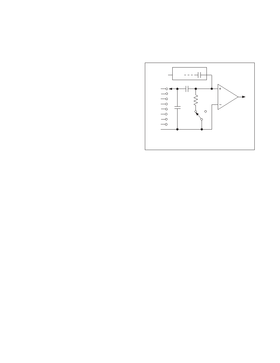
Pseudo-Differential Input
The sampling architecture of the ADC’s analog com-
parator is illustrated in the Equivalent Input Circuit
(Figure 4). In single-ended mode, IN+ is internally
switched to CH0-CH7 and IN- is switched to AGND. In
differential mode, IN+ and IN- are selected from pairs
of CH0/CH1, CH2/CH3, CH4/CH5 and CH6/CH7.
Configure the channels with Table 3 and Table 4.
In differential mode, IN- and IN+ are internally switched
to either one of the analog inputs. This configuration is
pseudo-differential to the effect that only the signal at
IN+ is sampled. The return side (IN-) must remain sta-
ble within ±0.5LSB (±0.1LSB for best results) with
respect to AGND during a conversion. Accomplish this
by connecting a 0.1F capacitor from AIN- (the select-
ed analog input, respectively) to AGND.
During the acquisition interval, the channel selected as
the positive input (IN+) charges capacitor CHOLD. The
acquisition interval spans three SCLK cycles and ends
on the falling SCLK edge after the last bit of the input
control word has been entered. At the end of the acqui-
sition interval, the T/H switch opens, retaining charge
on CHOLD as a sample of the signal at IN+.
The conversion interval begins with the input multiplex-
er switching CHOLD from the positive input (IN+) to the
negative input (IN-). In single-ended mode, IN- is sim-
ply AGND. This unbalances node ZERO at the input of
the comparator. The capacitive DAC adjusts during the
remainder of the conversion cycle to restore node
ZERO to 0V within the limits of 12-bit resolution. This
action is equivalent to transferring a charge of 16pF x
[(VIN+) - (VIN-)] from CHOLD to the binary-weighted
capacitive DAC, which in turn forms a digital represen-
tation of the analog input signal.
Track/Hold
The T/H enters its tracking mode on the falling clock
edge after the fifth bit of the 8-bit control word has been
shifted in. The T/H enters its hold mode on the falling
clock edge after the eighth bit of the control word has
been shifted in. If the converter is set up for
single-ended inputs, IN- is connected to AGND, and
the converter samples the “+” input. If the converter is
set up for differential inputs, IN- connects to the “-”
input, and the difference of
|IN+ - IN-| is sampled. At
the end of the conversion, the positive input connects
back to IN+, and CHOLD charges to the input signal.
The time required for the T/H to acquire an input signal
is a function of how quickly its input capacitance is
charged. If the input signal’s source impedance is high,
the acquisition time lengthens and more time must be
allowed between conversions. Acquisition time is cal-
culated by:
tAZ = 9 x (RS + RIN) x 16pF,
where RIN = 5kΩ, RS = the source impedance of the
input signal, and tAZ is never less than 1.5s. Note that
source impedances below 5k
Ω do not significantly
affect the AC performance of the ADC. Higher source
impedances can be used if an input capacitor is con-
nected to the analog inputs, as shown in Figure 5. Note
that the input capacitor forms an RC filter with the input
source impedance, limiting the ADC’s signal bandwidth.
Input Bandwidth
The ADC’s input tracking circuitry has a 4.5MHz
small-signal bandwidth, so it is possible to digitize
high-speed transient events and measure periodic sig-
nals with bandwidths exceeding the ADC’s sampling
rate by using undersampling techniques. To avoid
high-frequency signals being aliased into the frequency
band of interest, anti-alias filtering is recommended.
Low-Power, 8-Channel,
Serial 12-Bit ADCs
8
Maxim Integrated
MAX186/MAX188
CH0
CH1
CH2
CH3
CH4
CH5
CH6
CH7
AGND
CSWITCH
TRACK
T/H
SWITCH
10k
Ω
RS
CHOLD
HOLD
12-BIT CAPACITIVE DAC
VREF
ZERO
COMPARATOR
–
+
16pF
SINGLE-ENDED MODE: IN+ = CHO-CH7, IN– = AGND.
DIFFERENTIAL MODE: IN+ AND IN– SELECTED FROM PAIRS OF
CH0/CH1, CH2/CH3, CH4/CH5, CH6/CH7.
AT THE SAMPLING INSTANT,
THE MUX INPUT SWITCHES
FROM THE SELECTED IN+
CHANNEL TO THE SELECTED
IN– CHANNEL.
INPUT
MUX
Figure 4. Equivalent Input Circuit
相关PDF资料 |
PDF描述 |
|---|---|
| VI-BWJ-MX-B1 | CONVERTER MOD DC/DC 36V 75W |
| VI-BW3-MX-B1 | CONVERTER MOD DC/DC 24V 75W |
| MAX181BEQH+TD | IC DAS 12BIT 100KSPS 44-PLCC |
| VI-B7Y-MX-S | CONVERTER MOD DC/DC 3.3V 49.5W |
| M83723/75R14157 | CONN PLUG 15POS STRAIGHT W/SCKT |
相关代理商/技术参数 |
参数描述 |
|---|---|
| MAX188ACAP+ | 功能描述:模数转换器 - ADC 12-Bit 8Ch 133ksps 5.25V Precision ADC RoHS:否 制造商:Texas Instruments 通道数量:2 结构:Sigma-Delta 转换速率:125 SPs to 8 KSPs 分辨率:24 bit 输入类型:Differential 信噪比:107 dB 接口类型:SPI 工作电源电压:1.7 V to 3.6 V, 2.7 V to 5.25 V 最大工作温度:+ 85 C 安装风格:SMD/SMT 封装 / 箱体:VQFN-32 |
| MAX188ACAP+T | 功能描述:模数转换器 - ADC 12-Bit 8Ch 133ksps 5.25V Precision ADC RoHS:否 制造商:Texas Instruments 通道数量:2 结构:Sigma-Delta 转换速率:125 SPs to 8 KSPs 分辨率:24 bit 输入类型:Differential 信噪比:107 dB 接口类型:SPI 工作电源电压:1.7 V to 3.6 V, 2.7 V to 5.25 V 最大工作温度:+ 85 C 安装风格:SMD/SMT 封装 / 箱体:VQFN-32 |
| MAX188ACAP-T | 功能描述:模数转换器 - ADC RoHS:否 制造商:Texas Instruments 通道数量:2 结构:Sigma-Delta 转换速率:125 SPs to 8 KSPs 分辨率:24 bit 输入类型:Differential 信噪比:107 dB 接口类型:SPI 工作电源电压:1.7 V to 3.6 V, 2.7 V to 5.25 V 最大工作温度:+ 85 C 安装风格:SMD/SMT 封装 / 箱体:VQFN-32 |
| MAX188ACPP | 功能描述:模数转换器 - ADC RoHS:否 制造商:Texas Instruments 通道数量:2 结构:Sigma-Delta 转换速率:125 SPs to 8 KSPs 分辨率:24 bit 输入类型:Differential 信噪比:107 dB 接口类型:SPI 工作电源电压:1.7 V to 3.6 V, 2.7 V to 5.25 V 最大工作温度:+ 85 C 安装风格:SMD/SMT 封装 / 箱体:VQFN-32 |
| MAX188ACPP+ | 功能描述:模数转换器 - ADC 12-Bit 8Ch 133ksps 5.25V Precision ADC RoHS:否 制造商:Texas Instruments 通道数量:2 结构:Sigma-Delta 转换速率:125 SPs to 8 KSPs 分辨率:24 bit 输入类型:Differential 信噪比:107 dB 接口类型:SPI 工作电源电压:1.7 V to 3.6 V, 2.7 V to 5.25 V 最大工作温度:+ 85 C 安装风格:SMD/SMT 封装 / 箱体:VQFN-32 |
发布紧急采购,3分钟左右您将得到回复。