- 您现在的位置:买卖IC网 > PDF目录13119 > MAX1917EEE+ (Maxim Integrated Products)IC CNTRLR SYNC BUCK 16-QSOP PDF资料下载
参数资料
| 型号: | MAX1917EEE+ |
| 厂商: | Maxim Integrated Products |
| 文件页数: | 12/18页 |
| 文件大小: | 0K |
| 描述: | IC CNTRLR SYNC BUCK 16-QSOP |
| 产品培训模块: | Lead (SnPb) Finish for COTS Obsolescence Mitigation Program |
| 标准包装: | 100 |
| 应用: | 控制器,DDR |
| 输入电压: | 4.5 V ~ 22 V |
| 输出数: | 2 |
| 输出电压: | 0.4 V ~ 5 V |
| 工作温度: | 0°C ~ 85°C |
| 安装类型: | 表面贴装 |
| 封装/外壳: | 16-SSOP(0.154",3.90mm 宽) |
| 供应商设备封装: | 16-QSOP |
| 包装: | 管件 |
�� �
�
�Tracking,� Sinking� and� Sourcing,� Synchronous� Buck�
�Controller� for� DDR� Memory� and� Termination� Supplies�
�high-side� FET� from� turning� on� until� DL� is� fully� off.� There�
�must� be� a� low-resistance,� low-inductance� path� from� the�
�DL� driver� to� the� MOSFET� gate� in� order� for� the� adaptive�
�dead-time� circuit� to� work� properly.� Otherwise,� the�
�sense� circuitry� in� the� MAX1917� interprets� the� MOSFET�
�gate� as� off� while� there� is� actually� still� charge� left� on� the�
�gate.� Use� very� short,� wide� traces� measuring� 10�
�squares� to� 20� squares� (50mils� to� 100mils� wide� if� the�
�MOSFET� is� 1in� from� the� MAX1917).� The� dead� time� at�
�the� other� edge� (DH� turning� off)� is� determined� by� a� fixed�
�35ns� (typ)� internal� delay.� The� internal� pulldown� transis-�
�tor� that� drives� DL� low� is� robust,� with� a� 0.5� ?� (typ)� on-�
�R2�
�resistance.� This� helps� prevent� DL� from� being� pulled� up�
�during� the� fast� rise� time� of� the� inductor� node,� due� to�
�capacitive� coupling� from� the� drain� to� the� gate� of� the�
�massive� low-side� synchronous-rectifier� MOSFET.� Some�
�combinations� of� high-� and� low-side� FETs� may� be�
�encountered� that� cause� excessive� gate-drain� coupling,�
�which� can� lead� to� efficiency-killing,� EMI-producing�
�shoot-through� currents.� This� can� often� be� remedied� by�
�adding� a� resistor� (R� BST� )� in� series� with� BST,� which�
�increases� the� turn-on� time� of� the� high-side� FET� without�
�degrading� the� turn-off� time� (Figure� 2).�
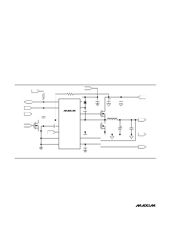
�Typical� Application� Circuits�
�VL�
�VL�
�5.1k� ?�
�POK�
�R3�
�20k� ?�
�3�
�POK�
�VL�
�11�
�D1�
�CMPSH-3�
�C3�
�4.7� μ� F�
�10V�
�C2�
�2� x� 330� μ� F�
�6V�
�C1�
�1� μ� F�
�6.3V�
�2.5V�
�V� IN�
�V+�
�V� DDR�
�5.5V� TO� 14V�
�C9�
�10�
�2�
�V+�
�DDR�
�MAX1917�
�BST�
�DH�
�14�
�15�
�C4�
�0.47� μ� F�
�10V�
�Q1�
�IRF7463�
�0.68� μ� H/9A�
�C6�
�SHDN�
�Q3�
�2N7002K�
�0.47� μ� F/25V�
�C8�
�0.47� μ� F/10V�
�VL�
�1�
�7�
�5�
�EN/HSD�
�REF�
�ILIM�
�LX�
�DL�
�PGND�
�16�
�12�
�13�
�2.5V�
�L1�
�Q2�
�IRF7463�
�6� x� 270� μ� F�
�2V�
�1.25V� AT� 7A�
�C5�
�2� x� 10� μ� F�
�6.3V�
�V� OUT�
�PGND�
�6�
�FSEL�
�VTT�
�4�
�8�
�GND�
�VTTR�
�9�
�C7�
�1� μ� F/6.3V�
�VTTR�
�OUTPUT� CAPACITORS� ARE� SELECTED� TO� COMPLY� WITH� JEDEC� SPECIFICATIONS.�
�Figure� 3.� Typical� Application� Circuit� for� 1.25V� at� 7A� Output�
�12�
�______________________________________________________________________________________�
�相关PDF资料 |
PDF描述 |
|---|---|
| VE-J1W-CZ-B1 | CONVERTER MINIMOD DC/DC 5.5V 25W |
| VI-J1W-CZ-B1 | CONVERTER MINIMOD DC/DC 5.5V 25W |
| 1782-19J | COIL RF .91UH MOLDED UNSHIELDED |
| HSC17DRYI-S13 | CONN EDGECARD 34POS .100 EXTEND |
| VI-B2J-EY-F3 | CONVERTER MOD DC/DC 36V 50W |
相关代理商/技术参数 |
参数描述 |
|---|---|
| MAX1917EEE+ | 功能描述:直流/直流开关转换器 Track/Sink/Source Synchronous Buck RoHS:否 制造商:STMicroelectronics 最大输入电压:4.5 V 开关频率:1.5 MHz 输出电压:4.6 V 输出电流:250 mA 输出端数量:2 最大工作温度:+ 85 C 安装风格:SMD/SMT |
| MAX1917EEE+T | 功能描述:直流/直流开关转换器 Track/Sink/Source Synchronous Buck RoHS:否 制造商:STMicroelectronics 最大输入电压:4.5 V 开关频率:1.5 MHz 输出电压:4.6 V 输出电流:250 mA 输出端数量:2 最大工作温度:+ 85 C 安装风格:SMD/SMT |
| MAX1917EEE-T | 功能描述:直流/直流开关转换器 RoHS:否 制造商:STMicroelectronics 最大输入电压:4.5 V 开关频率:1.5 MHz 输出电压:4.6 V 输出电流:250 mA 输出端数量:2 最大工作温度:+ 85 C 安装风格:SMD/SMT |
| MAX1917EEE-TG068 | 制造商:Rochester Electronics LLC 功能描述: 制造商:Maxim Integrated Products 功能描述: |
| MAX1917EVKIT | 功能描述:电源管理IC开发工具 RoHS:否 制造商:Maxim Integrated 产品:Evaluation Kits 类型:Battery Management 工具用于评估:MAX17710GB 输入电压: 输出电压:1.8 V |
发布紧急采购,3分钟左右您将得到回复。