- 您现在的位置:买卖IC网 > PDF目录10489 > MAX191ACWG+ (Maxim Integrated Products)IC ADC 12BIT 100KSPS 24-SOIC PDF资料下载
参数资料
| 型号: | MAX191ACWG+ |
| 厂商: | Maxim Integrated Products |
| 文件页数: | 10/24页 |
| 文件大小: | 0K |
| 描述: | IC ADC 12BIT 100KSPS 24-SOIC |
| 产品培训模块: | Lead (SnPb) Finish for COTS Obsolescence Mitigation Program |
| 标准包装: | 30 |
| 位数: | 12 |
| 采样率(每秒): | 100k |
| 数据接口: | MICROWIRE?,并联,QSPI?,串行,SPI? |
| 转换器数目: | 1 |
| 功率耗散(最大): | 941mW |
| 电压电源: | 双 ± |
| 工作温度: | 0°C ~ 70°C |
| 安装类型: | 表面贴装 |
| 封装/外壳: | 24-SOIC(0.295",7.50mm 宽) |
| 供应商设备封装: | 24-SOIC W |
| 包装: | 管件 |
| 输入数目和类型: | 2 个单端,单极;2 个单端,双极;1 个差分,单极;1 个差分,双极 |
MAX191
Following the data transfer, the DSP receive shift regis-
ter (RSR) contains a 16-bit word consisting of the 12
data bits, MSB first, followed by four trailing 0s.
Applications Information
Power-On Initialization
When the +5V power supply is first applied to the
MAX191, perform a single conversion to initialize the
ADC (the BUSY signal status is undefined at power-on).
Disregard the data outputs.
Power-Down Mode
In some battery-powered systems, it is desirable to
power down or remove power from the ADC during
inactive periods. To power down the MAX191, drive PD
low. In this mode, all internal ADC circuitry is off except
the reference, and the ADC consumes less than 50A
max (assuming all signals CS, RD, CLK, and HBEN are
static and within 200mV of the supplies). Figure 17
shows a practical way to drive the PD pin. If using inter-
nal reference compensation, drive PD between VDD
and DGND with a P I/O pin or other logic device
(Figure 17a). For external-reference compensation
mode, use the circuit in Figure 17b to drive PD between
DGND and the floating voltage of PD. An alternative is
to drive PD with three-state logic or a switch, provided
the off leakage does not exceed 100nA.
Internal Reference
The internal 4.096V reference is available at VREF and
must be bypassed to AGND with a 4.7F low-ESR
capacitor (less than 1/2
) in parallel with a 0.1F capaci-
tor, unless internal-reference compensation mode is
used (see the
Internal Reference Compensation section).
This minimizes noise and maintains a low reference
impedance at high frequencies. The reference output
can be disabled by connecting REFADJ to VDD when
using an external reference.
Reference-Compensation Modes
Power-down performance can be optimized for a given
conversion rate by selecting either internal or external
reference compensation.
Internal Compensation
The connection for internal compensation is shown in
Figure 18a. In this mode, the reference stabilizes quick-
ly enough so that a conversion typically starts within
35s after the ADC is reactivated (PD pulled high). In
this compensation mode, the reference buffer requires
longer recovery time from SAR transients, therefore
requiring a slower clock (and conversion time). With
internal reference compensation, the typical conversion
time rises to 25s (Figure 18b). Figure 18c illustrates
the typical average supply current vs. conversion rate,
Low-Power, 12-Bit Sampling ADC
with Internal Reference and Power-Down
18
______________________________________________________________________________________
MAX191
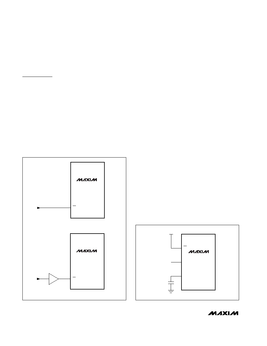
a. INTERNAL-REFERENCE COMPENSATION MODE
b. EXTERNAL-REFERENCE COMPENSATION MODE
PD
1
PD
OPEN-DRAIN
BUFFER
Figure 17. Drive Circuits for PD Pin
MAX191
+5V
PD
VREF
REFADJ
0.1
F
1
5
6
Figure 18a. Internal-Compensation Mode Circuit
相关PDF资料 |
PDF描述 |
|---|---|
| MS3101E12S-3S | CONN RCPT 2POS FREE HNG W/SCKT |
| VE-23N-IV-B1 | CONVERTER MOD DC/DC 18.5V 150W |
| MS3102A22-12S | CONN RCPT 5POS BOX MNT W/SCKT |
| EXP-0921/07/P | CONN RCPT 7POS IP68 W/PINS |
| MAX122BCAG+ | IC ADC 12BIT 333KSPS 24-SSOP |
相关代理商/技术参数 |
参数描述 |
|---|---|
| MAX191ACWG+ | 功能描述:模数转换器 - ADC 12Bit 100ksps 5V Precision ADC RoHS:否 制造商:Texas Instruments 通道数量:2 结构:Sigma-Delta 转换速率:125 SPs to 8 KSPs 分辨率:24 bit 输入类型:Differential 信噪比:107 dB 接口类型:SPI 工作电源电压:1.7 V to 3.6 V, 2.7 V to 5.25 V 最大工作温度:+ 85 C 安装风格:SMD/SMT 封装 / 箱体:VQFN-32 |
| MAX191ACWG+T | 功能描述:模数转换器 - ADC 12Bit 100ksps 5V Precision ADC RoHS:否 制造商:Texas Instruments 通道数量:2 结构:Sigma-Delta 转换速率:125 SPs to 8 KSPs 分辨率:24 bit 输入类型:Differential 信噪比:107 dB 接口类型:SPI 工作电源电压:1.7 V to 3.6 V, 2.7 V to 5.25 V 最大工作温度:+ 85 C 安装风格:SMD/SMT 封装 / 箱体:VQFN-32 |
| MAX191ACWG-T | 功能描述:模数转换器 - ADC RoHS:否 制造商:Texas Instruments 通道数量:2 结构:Sigma-Delta 转换速率:125 SPs to 8 KSPs 分辨率:24 bit 输入类型:Differential 信噪比:107 dB 接口类型:SPI 工作电源电压:1.7 V to 3.6 V, 2.7 V to 5.25 V 最大工作温度:+ 85 C 安装风格:SMD/SMT 封装 / 箱体:VQFN-32 |
| MAX191AENG | 功能描述:模数转换器 - ADC RoHS:否 制造商:Texas Instruments 通道数量:2 结构:Sigma-Delta 转换速率:125 SPs to 8 KSPs 分辨率:24 bit 输入类型:Differential 信噪比:107 dB 接口类型:SPI 工作电源电压:1.7 V to 3.6 V, 2.7 V to 5.25 V 最大工作温度:+ 85 C 安装风格:SMD/SMT 封装 / 箱体:VQFN-32 |
| MAX191AENG+ | 功能描述:模数转换器 - ADC RoHS:否 制造商:Texas Instruments 通道数量:2 结构:Sigma-Delta 转换速率:125 SPs to 8 KSPs 分辨率:24 bit 输入类型:Differential 信噪比:107 dB 接口类型:SPI 工作电源电压:1.7 V to 3.6 V, 2.7 V to 5.25 V 最大工作温度:+ 85 C 安装风格:SMD/SMT 封装 / 箱体:VQFN-32 |
发布紧急采购,3分钟左右您将得到回复。