- 您现在的位置:买卖IC网 > PDF目录383341 > MAX192ACAP (MAXIM INTEGRATED PRODUCTS INC) Fixed-Point Digital Signal Processor 288-FCBGA PDF资料下载
参数资料
| 型号: | MAX192ACAP |
| 厂商: | MAXIM INTEGRATED PRODUCTS INC |
| 元件分类: | ADC |
| 英文描述: | Fixed-Point Digital Signal Processor 288-FCBGA |
| 中文描述: | 8-CH 10-BIT SUCCESSIVE APPROXIMATION ADC, SERIAL ACCESS, PDSO20 |
| 封装: | 5.30 MM, 0.65 MM PITCH, SSOP-20 |
| 文件页数: | 12/24页 |
| 文件大小: | 201K |
| 代理商: | MAX192ACAP |
M
Low-Power, 8-Channel,
S erial 10-Bit ADC
12
______________________________________________________________________________________
SSTRB
CS
SCLK
DIN
DOUT
1
4
8
12
16
20
24
START
SEL2 SEL1 SEL0
BIP
DIF
PD1
PD0
B9
B8
B7
B6
B5
B4
B3
B2
B1
B0
S1
SO
ACQUISITION
1.5μs (CLK = 2MHz)
IDLE
FILLED WITH
ZEROS
IDLE
CONVERSION
t
ACQ
A/D STATE
RB1
RB1
RB2
RB3
RB2
RB3
CS
SCLK
DIN
DOUT
t
CSH
t
CSS
t
CL
t
DS
t
DH
t
DV
t
CH
t
DO
t
TR
t
CSH
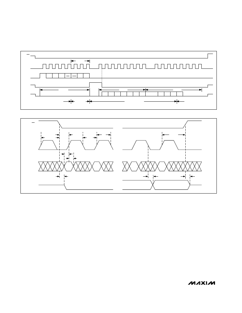
Figure 6. 24-Bit External Clock Mode Conversion Timing (SPI, QSPI and Microwire Compatible)
Figure 7. Detailed Serial-Interface Timing
Pulling
CS
high prevents data from being clocked into
the MAX192 and three-states DOUT, but it does not
adversely affect an internal clock-mode conversion
already in progress. When internal clock mode is
selected, SSTRB does not go into a high-impedance
state when
CS
goes high.
Figure 10 shows the SSTRB timing in internal clock
mode. In internal clock mode, data can be shifted in
and out of the MAX192 at clock rates exceeding
4.0MHz, provided that the minimum acquisition time,
t
AZ
, is kept above 1.5μs.
Data Framing
The falling edge of
CS
does
not
start a conversion on
the MAX192. The first logic high clocked into DIN is inter-
preted as a start bit and defines the first bit of the control
byte. A conversion starts on the falling edge of SCLK,
after the eighth bit of the control byte (the PD0 bit) is
clocked into DIN. The start bit is defined as:
The first high bit clocked into DIN with
CS
low any-
time the converter is idle, e.g. after V
DD
is applied.
OR
The first high bit clocked into DIN after bit 3 of a
conversion in progress is clocked onto the DOUT pin.
If a falling edge on
CS
forces a start bit before bit 3
(B3) becomes available, then the current conversion
will be terminated and a new one started. Thus, the
fastest the MAX192 can run is 15 clocks per conver-
sion. Figure 11a shows the serial-interface timing nec-
essary to perform a conversion every 15 SCLK cycles
in external clock mode. If
CS
is low and SCLK is contin-
uous, guarantee a start bit by first clocking in 16 zeros.
相关PDF资料 |
PDF描述 |
|---|---|
| MAX192ACPP | Fixed-Point Digital Signal Processor 288-FCBGA |
| MAX192ACWP | Fixed-Point Digital Signal Processor 288-FCBGA |
| MAX192AEPP | |
| MAX192BCAP | Low-Power, 8-Channel, Serial 10-Bit ADC |
| MAX192BEAP | Low-Power, 8-Channel, Serial 10-Bit ADC |
相关代理商/技术参数 |
参数描述 |
|---|---|
| MAX192ACAP+ | 功能描述:模数转换器 - ADC 10-Bit 8Ch 133ksps 5V Precision ADC RoHS:否 制造商:Texas Instruments 通道数量:2 结构:Sigma-Delta 转换速率:125 SPs to 8 KSPs 分辨率:24 bit 输入类型:Differential 信噪比:107 dB 接口类型:SPI 工作电源电压:1.7 V to 3.6 V, 2.7 V to 5.25 V 最大工作温度:+ 85 C 安装风格:SMD/SMT 封装 / 箱体:VQFN-32 |
| MAX192ACAP+T | 功能描述:模数转换器 - ADC 10-Bit 8Ch 133ksps 5V Precision ADC RoHS:否 制造商:Texas Instruments 通道数量:2 结构:Sigma-Delta 转换速率:125 SPs to 8 KSPs 分辨率:24 bit 输入类型:Differential 信噪比:107 dB 接口类型:SPI 工作电源电压:1.7 V to 3.6 V, 2.7 V to 5.25 V 最大工作温度:+ 85 C 安装风格:SMD/SMT 封装 / 箱体:VQFN-32 |
| MAX192ACAP-T | 功能描述:模数转换器 - ADC RoHS:否 制造商:Texas Instruments 通道数量:2 结构:Sigma-Delta 转换速率:125 SPs to 8 KSPs 分辨率:24 bit 输入类型:Differential 信噪比:107 dB 接口类型:SPI 工作电源电压:1.7 V to 3.6 V, 2.7 V to 5.25 V 最大工作温度:+ 85 C 安装风格:SMD/SMT 封装 / 箱体:VQFN-32 |
| MAX192ACPP | 功能描述:模数转换器 - ADC RoHS:否 制造商:Texas Instruments 通道数量:2 结构:Sigma-Delta 转换速率:125 SPs to 8 KSPs 分辨率:24 bit 输入类型:Differential 信噪比:107 dB 接口类型:SPI 工作电源电压:1.7 V to 3.6 V, 2.7 V to 5.25 V 最大工作温度:+ 85 C 安装风格:SMD/SMT 封装 / 箱体:VQFN-32 |
| MAX192ACPP+ | 功能描述:模数转换器 - ADC 10-Bit 8Ch 133ksps 5V Precision ADC RoHS:否 制造商:Texas Instruments 通道数量:2 结构:Sigma-Delta 转换速率:125 SPs to 8 KSPs 分辨率:24 bit 输入类型:Differential 信噪比:107 dB 接口类型:SPI 工作电源电压:1.7 V to 3.6 V, 2.7 V to 5.25 V 最大工作温度:+ 85 C 安装风格:SMD/SMT 封装 / 箱体:VQFN-32 |
发布紧急采购,3分钟左右您将得到回复。