- 您现在的位置:买卖IC网 > PDF目录1841 > MAX1931EUB+T (Maxim Integrated Products)IC SW CUR LIMIT USB 10-UMAX PDF资料下载
参数资料
| 型号: | MAX1931EUB+T |
| 厂商: | Maxim Integrated Products |
| 文件页数: | 7/8页 |
| 文件大小: | 0K |
| 描述: | IC SW CUR LIMIT USB 10-UMAX |
| 产品培训模块: | Lead (SnPb) Finish for COTS Obsolescence Mitigation Program |
| 标准包装: | 2,500 |
| 应用: | USB,外设 |
| 电流 - 电源: | 14µA |
| 电源电压: | 2.7 V ~ 5.5 V |
| 工作温度: | -40°C ~ 85°C |
| 安装类型: | 表面贴装 |
| 封装/外壳: | 10-TFSOP,10-MSOP(0.118",3.00mm 宽) |
| 供应商设备封装: | 10-µMAX |
| 包装: | 带卷 (TR) |
�� �
�
�Current-Limited� Switch� for� Single� USB� Port�
�spurious� FAULT� output.� Load-transient� faults� less� than�
�10ms� (typ)� do� not� cause� a� FAULT� output� assertion.�
�Only� current-limit� faults� are� blanked.� Die� overtempera-�
�ture� faults� and� input� voltage� droops� below� the� UVLO�
�threshold� cause� an� immediate� fault� output.�
�Applications� Information�
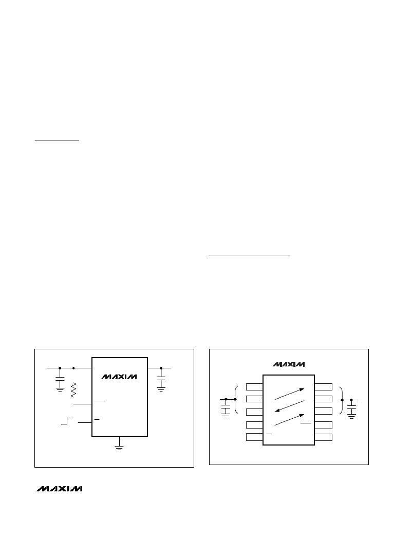
�Input� Capacitor�
�To� limit� the� input� voltage� drop� during� momentary� output�
�short-circuit� conditions,� connect� a� capacitor� from� IN� to�
�GND.� A� 1μF� ceramic� capacitor� is� adequate� for� most�
�applications;� however,� higher� capacitor� values� further�
�reduce� the� voltage� drop� at� the� input� (see� Figure� 2).�
�Output� Capacitor�
�Connect� a� 0.1μF� capacitor� from� OUT� to� GND.� This� cap-�
�acitor� helps� prevent� inductive� parasitics� from� pulling�
�OUT� negative� during� turn-off.�
�Layout� and� Thermal� Dissipation�
�To� optimize� the� switch-response� time� to� output� short-�
�circuit� conditions,� it� is� very� important� to� keep� all� traces�
�as� short� as� possible� to� reduce� the� effect� of� undesirable�
�parasitic� inductance.� Place� input� and� output� capacitors�
�as� close� to� the� device� as� possible� (no� more� than� 5mm).�
�INPUT�
�All� IN� and� all� OUT� pins� must� be� connected� with� short�
�traces� to� the� power� bus.� Wide� power� bus� planes� pro-�
�vide� superior� heat� dissipation� through� the� switch� IN� and�
�OUT� pins.� Figure� 3� shows� suggested� pin� connections�
�for� a� single-layer� board.�
�Under� normal� operating� conditions,� the� package� can�
�dissipate� and� channel� heat� away.� Calculate� the� maxi-�
�mum� power� dissipation� as� follows:�
�P� =� (I� LIMIT� )� 2� ?� R� ON�
�where� I� LIMIT� is� the� preset� current� limit� (1.1A� max)� and�
�R� ON� is� the� on-resistance� of� the� switch� (150m� ?� max).�
�When� the� output� is� short-circuited,� foldback-current-lim-�
�iting� activates� and� the� voltage� drop� across� the� switch�
�equals� the� input� supply.� The� power� dissipated� across�
�the� switch� increases,� as� does� the� die� temperature.� If� the�
�fault� condition� is� not� removed,� the� thermal-overload� pro-�
�tection� circuitry� activates� (see� the� Thermal� Shutdown�
�section).� Wide� power-bus� planes� connected� to� IN� and�
�OUT� and� a� ground� plane� in� contact� with� the� device�
�help� dissipate� additional� heat.�
�Chip� Information�
�TRANSISTOR� COUNT:� 715�
�2.7V� TO� 5.5V�
�IN�
�OUT�
�OUTPUT�
�MAX1931�
�1� μ� F�
�0.1� μ� F*�
�OFF�
�100k� ?�
�FAULT�
�MAX1931�
�1�
�2�
�3�
�IN�
�OUT�
�IN�
�OUT�
�IN�
�OUT�
�10�
�9�
�8�
�ON�
�ON�
�4�
�OUT�
�FAULT�
�7�
�GND�
�5�
�ON�
�GND�
�6�
�*USB� SPECIFICATIONS� REQUIRE� A� LARGER� CAPACITOR�
�Figure� 2.� Typical� Application� Circuit�
�Figure� 3.� IN� and� OUT� Cross� Connections� for� a� Single-Layer�
�Board�
�_______________________________________________________________________________________�
�7�
�相关PDF资料 |
PDF描述 |
|---|---|
| MAX1932ETC+T | IC SUPPLY BIAS APD 12-TQFN |
| MAX1935ETA+T | IC REG LDO ADJ .5A 8TDFN |
| MAX1937EEI+T | IC REG CTRLR PWM HYBRID 28-QSOP |
| MAX1940EEE+ | IC SW USB TRPL 16-QSOP |
| MAX1945REUI+T | IC REG BUCK 6A 28TSSOP |
相关代理商/技术参数 |
参数描述 |
|---|---|
| MAX1932ETC | 功能描述:电流和电力监控器、调节器 RoHS:否 制造商:STMicroelectronics 产品:Current Regulators 电源电压-最大:48 V 电源电压-最小:5.5 V 工作温度范围:- 40 C to + 150 C 安装风格:SMD/SMT 封装 / 箱体:HPSO-8 封装:Reel |
| MAX1932ETC/GG8 | 功能描述:电流和电力监控器、调节器 RoHS:否 制造商:STMicroelectronics 产品:Current Regulators 电源电压-最大:48 V 电源电压-最小:5.5 V 工作温度范围:- 40 C to + 150 C 安装风格:SMD/SMT 封装 / 箱体:HPSO-8 封装:Reel |
| MAX1932ETC+ | 功能描述:其他电源管理 0.5% Accurate APD Bias Supply RoHS:否 制造商:Texas Instruments 输出电压范围: 输出电流:4 mA 输入电压范围:3 V to 3.6 V 输入电流: 功率耗散: 工作温度范围:- 40 C to + 110 C 安装风格:SMD/SMT 封装 / 箱体:VQFN-48 封装:Reel |
| MAX1932ETC+ | 制造商:Maxim Integrated Products 功能描述:SUPPLY BIAS APD SMD 1932 TQFN12 制造商:Maxim Integrated Products 功能描述:SUPPLY BIAS, APD, SMD, 1932, TQFN12 |
| MAX1932ETC+T | 功能描述:其他电源管理 0.5% Accurate APD Bias Supply RoHS:否 制造商:Texas Instruments 输出电压范围: 输出电流:4 mA 输入电压范围:3 V to 3.6 V 输入电流: 功率耗散: 工作温度范围:- 40 C to + 110 C 安装风格:SMD/SMT 封装 / 箱体:VQFN-48 封装:Reel |
发布紧急采购,3分钟左右您将得到回复。