- 您现在的位置:买卖IC网 > PDF目录13133 > MAX1932ETC+ (Maxim Integrated Products)IC SUPPLY BIAS APD 12-TQFN PDF资料下载
参数资料
| 型号: | MAX1932ETC+ |
| 厂商: | Maxim Integrated Products |
| 文件页数: | 6/16页 |
| 文件大小: | 0K |
| 描述: | IC SUPPLY BIAS APD 12-TQFN |
| 产品培训模块: | Lead (SnPb) Finish for COTS Obsolescence Mitigation Program |
| 标准包装: | 75 |
| 应用: | 控制器,光纤网络 |
| 输入电压: | 2.7 V ~ 5.5 V |
| 输出数: | 1 |
| 输出电压: | 4.5 V ~ 90 V |
| 工作温度: | 0°C ~ 85°C |
| 安装类型: | 表面贴装 |
| 封装/外壳: | 12-WQFN 裸露焊盘 |
| 供应商设备封装: | 12-TQFN-EP(4x4) |
| 包装: | 管件 |
| 产品目录页面: | 1410 (CN2011-ZH PDF) |
�� �
�
�Digitally� Controlled,� 0.5%� Accurate,�
�Safest� APD� Bias� Supply�
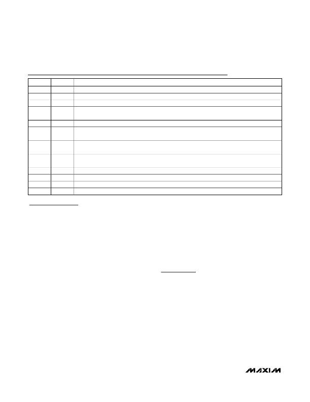
�Pin� Description�
�PIN�
�1�
�2�
�3�
�4�
�5�
�6�
�7�
�8�
�9�
�10�
�11�
�12�
�NAME�
�SCLK�
�DIN�
�CL�
�CS+�
�CS-�
�DACOUT�
�FB�
�COMP�
�GND�
�GATE�
�VIN�
�CS�
�FUNCTION�
�DAC� Serial� Clock� Input�
�DAC� Serial� Data� Input�
�Current-Limit� Indicator� Flag.� CL� =� 0� indicates� that� the� part� is� in� current� limit.� Logic� high� level� =� VIN.�
�Current-Limit� Plus� Sense� Input.� Connect� a� resistor� from� CS+� to� CS-� in� series� with� the� output.� The� differential�
�threshold� is� 2V.� CS+� has� typically� 1M� Ω� resistance� to� ground.�
�Current-Limit� Minus� Sense� Input.� CS-� has� typically� 1M� Ω� resistance� to� ground.�
�Internal� DAC� Output.� Generates� a� control� voltage� for� adjustable� output� operation.� DACOUT� can� source� or�
�sink� 50μA.�
�Feedback� input.� Connect� to� a� resistive� voltage-divider� between� the� output� voltage� (V� OUT� )� and� FB� to� set� the�
�output� voltage.� The� feedback� set� point� is� 1.25V.�
�Compensation� Pin.� Compensates� the� DC-DC� converter� control� loop� with� a� series� RC� to� GND.� COMP� is�
�actively� discharged� to� ground� during� shutdown� or� undervoltage� conditions.�
�Ground�
�Gate-Driver� Output� for� External� N-FET�
�IC� Supply� Voltage� (2.7V� to� 5.5V).� Bypass� VIN� with� a� 1μF� or� greater� ceramic� capacitor.�
�DAC� Chip-Select� Input�
�Detailed� Description�
�Fixed� Frequency� PWM�
�The� MAX1932� uses� a� constant� frequency,� PWM,� con-�
�troller� architecture.� This� controller� sets� the� switch� on-�
�time� and� drives� an� external� N-channel� MOSFET� (see�
�Figure� 1).� As� the� load� varies,� the� error� amplifier� sets� the�
�inductor� peak� current� necessary� to� supply� the� load� and�
�regulate� the� output� voltage.�
�Output� Current� Limit�
�The� MAX1932� uses� an� external� resistor� at� CS+� and� CS-�
�to� sense� the� output� current� (see� Figure� 2).� The� typical�
�current-limit� threshold� is� 2V.� CL� is� designed� to� help� find�
�the� optimum� APD� bias� point� by� going� low� to� indicate�
�when� the� APD� reaches� avalanche� and� that� current� limit�
�has� been� activated.� To� minimize� noise,� CL� only�
�changes� state� on� an� internal� oscillator� edge.�
�Output� Control� DAC�
�An� internal� digital-to-analog� converter� can� be� used� to�
�control� the� output� voltage� of� the� DC-DC� converter�
�(Figure� 2).� The� DAC� output� is� changed� through� an� SPI?�
�serial� interface� using� an� 8-bit� control� byte.� On� power-up,�
�the� DAC� defaults� to� FF� hex� (1.25V),� which� corresponds�
�to� a� minimum� boost� converter� output� voltage.�
�Alternately,� the� output� voltage� can� be� set� with� external�
�resistors,� an� external� DAC,� or� a� voltage� source.� Output�
�span� and� offset� are� independently� settable� with� exter-�
�SPI� is� a� trademark� of� Motorola,� Inc.�
�nal� resistors.� See� the� Applications� Information� section�
�for� output� control� equations.�
�SPI� Interface/Shutdown�
�Use� an� SPI-compatible� 3-wire� serial� interface� with� the�
�MAX1932� to� control� the� DAC� output� voltage� and� to� shut�
�down� the� MAX1932.� Figures� 4� and� 5� show� timing� diagrams�
�for� the� SPI� protocol.� The� MAX1932� is� a� write-only� device�
�and� uses� CS� along� with� SCLK� and� DIN� to� communicate.�
�The� serial� port� is� always� operational� when� the� device� is�
�powered.� To� shut� down� the� DC-DC� converter� portion� only,�
�update� the� DAC� registers� to� 00� hex.�
�Applications� Information�
�Voltage� Feedback� Sense� Point�
�Feedback� can� be� taken� from� in� front� of,� or� after,� the� cur-�
�rent-limit� sense� resistor.� The� current-limit� sense� resistor�
�forms� a� lowpass� filter� with� the� output� capacitor.� Taking�
�feedback� after� the� current-limit� sense� resistor� (see� Figure�
�2),� optimizes� the� output� voltage� accuracy,� but� requires�
�overcompensation,� which� slows� down� the� control� loop�
�response.� For� faster� response,� the� feedback� can� be�
�taken� from� in� front� of� the� current-sense� resistor� (see�
�Figure� 3).� This� configuration� however,� makes� the� output�
�voltage� more� sensitive� to� load� variation� and� degrades�
�output� accuracy� by� an� amount� equal� to� the� load� current�
�times� the� current-sense� resistor� value.�
�6�
�_______________________________________________________________________________________�
�相关PDF资料 |
PDF描述 |
|---|---|
| VE-B6H-EU | CONVERTER MOD DC/DC 52V 200W |
| VI-B1B-EU-F2 | CONVERTER MOD DC/DC 95V 200W |
| 450VXR56MEFCSN25X25 | CAP ALUM 56UF 450V 20% SNAP-IN |
| 1945-07K | COIL RF 8.2UH MOLDED UNSHIELDED |
| VE-B64-EU | CONVERTER MOD DC/DC 48V 200W |
相关代理商/技术参数 |
参数描述 |
|---|---|
| MAX1932ETC/GG8 | 功能描述:电流和电力监控器、调节器 RoHS:否 制造商:STMicroelectronics 产品:Current Regulators 电源电压-最大:48 V 电源电压-最小:5.5 V 工作温度范围:- 40 C to + 150 C 安装风格:SMD/SMT 封装 / 箱体:HPSO-8 封装:Reel |
| MAX1932ETC+ | 功能描述:其他电源管理 0.5% Accurate APD Bias Supply RoHS:否 制造商:Texas Instruments 输出电压范围: 输出电流:4 mA 输入电压范围:3 V to 3.6 V 输入电流: 功率耗散: 工作温度范围:- 40 C to + 110 C 安装风格:SMD/SMT 封装 / 箱体:VQFN-48 封装:Reel |
| MAX1932ETC+ | 制造商:Maxim Integrated Products 功能描述:SUPPLY BIAS APD SMD 1932 TQFN12 制造商:Maxim Integrated Products 功能描述:SUPPLY BIAS, APD, SMD, 1932, TQFN12 |
| MAX1932ETC+T | 功能描述:其他电源管理 0.5% Accurate APD Bias Supply RoHS:否 制造商:Texas Instruments 输出电压范围: 输出电流:4 mA 输入电压范围:3 V to 3.6 V 输入电流: 功率耗散: 工作温度范围:- 40 C to + 110 C 安装风格:SMD/SMT 封装 / 箱体:VQFN-48 封装:Reel |
| MAX1932ETC-T | 功能描述:其他电源管理 RoHS:否 制造商:Texas Instruments 输出电压范围: 输出电流:4 mA 输入电压范围:3 V to 3.6 V 输入电流: 功率耗散: 工作温度范围:- 40 C to + 110 C 安装风格:SMD/SMT 封装 / 箱体:VQFN-48 封装:Reel |
发布紧急采购,3分钟左右您将得到回复。