- 您现在的位置:买卖IC网 > PDF目录383342 > MAX194AEWE (MAXIM INTEGRATED PRODUCTS INC) Circular Connector; No. of Contacts:22; Series:MS27467; Body Material:Aluminum; Connecting Termination:Crimp; Connector Shell Size:13; Circular Contact Gender:Socket; Circular Shell Style:Straight Plug; Insert Arrangement:13-35 RoHS Compliant: No PDF资料下载
参数资料
| 型号: | MAX194AEWE |
| 厂商: | MAXIM INTEGRATED PRODUCTS INC |
| 元件分类: | ADC |
| 英文描述: | Circular Connector; No. of Contacts:22; Series:MS27467; Body Material:Aluminum; Connecting Termination:Crimp; Connector Shell Size:13; Circular Contact Gender:Socket; Circular Shell Style:Straight Plug; Insert Arrangement:13-35 RoHS Compliant: No |
| 中文描述: | 1-CH 14-BIT SUCCESSIVE APPROXIMATION ADC, SERIAL ACCESS, PDSO16 |
| 封装: | SO-16 |
| 文件页数: | 5/24页 |
| 文件大小: | 223K |
| 代理商: | MAX194AEWE |
_______________Detailed Desc ription
The MAX194 uses a successive-approximation register
(SAR) to convert an analog input to a 14-bit digital
code, which outputs as a serial data stream. The data
bits can be read either during the conversion, at the
CLK clock rate, or between conversions asynchronous
with CLK, at the SCLK rate (up to 5Mbps).
The MAX194 includes a capacitive digital-to-analog
converter (DAC) that provides an inherent track/hold
input. The interface and control logic are designed for
easy connection to most microprocessors (μPs), limiting
the need for external components. In addition to the
SAR and DAC, the MAX194 includes a serial interface, a
sampling comparator used by the SAR, ten calibration
DACs, and control logic for calibration and conversion.
The DAC consists of an array of capacitors with binary
weighted values plus one “dummy sub-LSB” capacitor
(Figure 1). During input acquisition in unipolar mode,
the array’s common terminal is connected to AGND
and all free terminals are connected to the input signal
(AIN). After acquisition, the common terminal is discon-
nected from AGND and the free terminals are discon-
nected from AIN, trapping a charge proportional to the
input voltage on the capacitor array.
The free terminal of the MSB (largest) capacitor is con-
nected to the reference (REF), which pulls the common
terminal (connected to the comparator) positive.
Simultaneously, the free terminals of all other capaci-
tors in the array are connected to AGND, which drives
the comparator input negative. If the analog input is
near V
REF
, connecting the MSB’s free terminal to REF
only pulls the comparator input slightly positive.
However, connecting the remaining capacitor’s free ter-
minals to ground drives the comparator input well
below ground, so that the comparator input is negative,
the comparator output is low, and the MSB is set high.
If the analog input is near ground, the comparator out-
put is high and the MSB is low.
Following this, the next largest capacitor is disconnect-
ed from AGND and connected to REF, and the com-
parator determines the next bit. This continues until all
bits have been determined. For a bipolar input range,
the MSB capacitor is connected to REF rather than AIN
during input acquisition, which results in an input range
of V
REF
to -V
REF
.
M
14-Bit, 85ksps ADC with 10μA S hutdown
_______________________________________________________________________________________
5
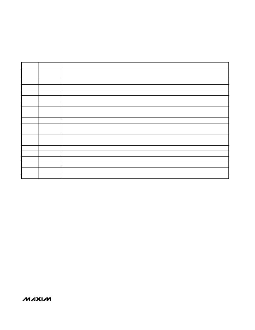
______________________________________________________________Pin Desc ription
PIN
NAME
FUNCTION
1
BP/UP/
SHDN
Bipolar/Unipolar/Shutdown Input. Three-state input selects bipolar or unipolar input range, or shutdown.
0V = shutdown, +5V = unipolar, floating = bipolar.
2
3
4
5
6
CLK
SCLK
VDDD
DOUT
DGND
Conversion Clock Input
Serial Clock Input is used to shift data out between conversions. May be asynchronous to CLK.
+5V Digital Power Supply
Serial Data Output, MSB first
Digital Ground
7
EOC
End-of-Conversion/Calibration Output—normally low. Rises at beginning of conversion or calibration and
falls at the end of either. May be used as an output framing signal.
8
CS
Chip-Select Input—active low. Enables the serial interface and the three-state data output (DOUT).
9
CONV
Convert-Start Input—active low. Conversion begins on the falling edge after
CONV
goes low if input signal
has been acquired; otherwise, on the falling clock edge after acquisition.
10
RESET
Reset Input. Pulling
RESET
low places ADC in inactive state. Rising edge resets control logic and begins
calibration.
11
12
13
14
15
16
VSSD
REF
AIN
AGND
VSSA
VDDA
-5V Digital Power Supply
Reference Input, 0 to 5V
Analog Input, 0 to V
REF
unipolar or ±V
REF
bipolar range
Analog Ground
-5V Analog Power Supply
+5V Analog Power Supply
相关PDF资料 |
PDF描述 |
|---|---|
| MAX194BCWE | 14-Bit, 85ksps ADC with 10A Shutdown |
| MAX194BCPE | 14-Bit, 85ksps ADC with 10A Shutdown |
| MAX194ACWE | 14-Bit, 85ksps ADC with 10A Shutdown |
| MAX194AEPE | Fixed-Point Digital Signal Processor 532-FCBGA |
| MAX194AMDE | 14-Bit, 85ksps ADC with 10A Shutdown |
相关代理商/技术参数 |
参数描述 |
|---|---|
| MAX194AEWE/GG8 | 功能描述:模数转换器 - ADC 14-Bit 85ksps ADC with 10uA Shutdown RoHS:否 制造商:Texas Instruments 通道数量:2 结构:Sigma-Delta 转换速率:125 SPs to 8 KSPs 分辨率:24 bit 输入类型:Differential 信噪比:107 dB 接口类型:SPI 工作电源电压:1.7 V to 3.6 V, 2.7 V to 5.25 V 最大工作温度:+ 85 C 安装风格:SMD/SMT 封装 / 箱体:VQFN-32 |
| MAX194AEWE+ | 功能描述:模数转换器 - ADC RoHS:否 制造商:Texas Instruments 通道数量:2 结构:Sigma-Delta 转换速率:125 SPs to 8 KSPs 分辨率:24 bit 输入类型:Differential 信噪比:107 dB 接口类型:SPI 工作电源电压:1.7 V to 3.6 V, 2.7 V to 5.25 V 最大工作温度:+ 85 C 安装风格:SMD/SMT 封装 / 箱体:VQFN-32 |
| MAX194AEWE+T | 功能描述:模数转换器 - ADC RoHS:否 制造商:Texas Instruments 通道数量:2 结构:Sigma-Delta 转换速率:125 SPs to 8 KSPs 分辨率:24 bit 输入类型:Differential 信噪比:107 dB 接口类型:SPI 工作电源电压:1.7 V to 3.6 V, 2.7 V to 5.25 V 最大工作温度:+ 85 C 安装风格:SMD/SMT 封装 / 箱体:VQFN-32 |
| MAX194AEWE-T | 功能描述:模数转换器 - ADC RoHS:否 制造商:Texas Instruments 通道数量:2 结构:Sigma-Delta 转换速率:125 SPs to 8 KSPs 分辨率:24 bit 输入类型:Differential 信噪比:107 dB 接口类型:SPI 工作电源电压:1.7 V to 3.6 V, 2.7 V to 5.25 V 最大工作温度:+ 85 C 安装风格:SMD/SMT 封装 / 箱体:VQFN-32 |
| MAX194AMDE | 功能描述:模数转换器 - ADC RoHS:否 制造商:Texas Instruments 通道数量:2 结构:Sigma-Delta 转换速率:125 SPs to 8 KSPs 分辨率:24 bit 输入类型:Differential 信噪比:107 dB 接口类型:SPI 工作电源电压:1.7 V to 3.6 V, 2.7 V to 5.25 V 最大工作温度:+ 85 C 安装风格:SMD/SMT 封装 / 箱体:VQFN-32 |
发布紧急采购,3分钟左右您将得到回复。