- 您现在的位置:买卖IC网 > PDF目录10753 > MAX19706ETM+ (Maxim Integrated Products)IC ANLG FRNT END 48-TQFN PDF资料下载
参数资料
| 型号: | MAX19706ETM+ |
| 厂商: | Maxim Integrated Products |
| 文件页数: | 19/37页 |
| 文件大小: | 0K |
| 描述: | IC ANLG FRNT END 48-TQFN |
| 产品培训模块: | Lead (SnPb) Finish for COTS Obsolescence Mitigation Program |
| 标准包装: | 43 |
| 位数: | 10 |
| 通道数: | 4 |
| 功率(瓦特): | 49.5mW |
| 电压 - 电源,模拟: | 2.7 V ~ 3.3 V |
| 电压 - 电源,数字: | 1.8 V ~ 3.3 V |
| 封装/外壳: | 48-WFQFN 裸露焊盘 |
| 供应商设备封装: | 48-TQFN-EP(7x7) |
| 包装: | 管件 |
第1页第2页第3页第4页第5页第6页第7页第8页第9页第10页第11页第12页第13页第14页第15页第16页第17页第18页当前第19页第20页第21页第22页第23页第24页第25页第26页第27页第28页第29页第30页第31页第32页第33页第34页第35页第36页第37页
MAX19706
10-Bit, 22Msps, Ultra-Low-Power
Analog Front-End
26
______________________________________________________________________________________
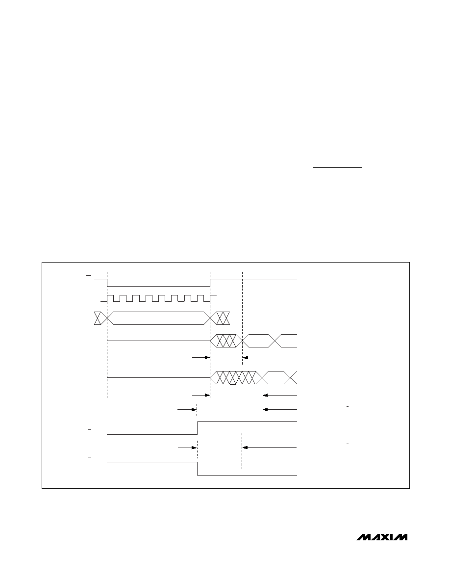
Mode-Recovery Timing
Figure 7 shows the mode-recovery timing diagram.
tWAKE is the wakeup time when exiting shutdown, idle,
or standby mode and entering Rx or Tx mode. tENABLE
is the recovery time when switching between either Rx
or Tx mode. tWAKE or tENABLE is the time for the Rx ADC
to settle within 1dB of specified SINAD performance and
Tx DAC settling to 10 LSB error. tWAKE and tENABLE
times are measured after either the 16-bit serial com-
mand is latched into the MAX19706 by a CS transition
high (SPI controlled) or a T/R logic transition (external
Tx-Rx control). In FAST mode, the recovery time is 0.5s
to switch between Tx or Rx modes.
System Clock Input (CLK)
Both the Rx ADC and Tx DAC share the CLK input. The
CLK input accepts a CMOS-compatible signal level set
by OVDD from 1.8V to VDD. Since the interstage con-
version of the device depends on the repeatability of
the rising and falling edges of the external clock, use a
clock with low jitter and fast rise and fall times (< 2ns).
Specifically, sampling occurs on the rising edge of the
clock signal, requiring this edge to provide the lowest
possible jitter. Any significant clock jitter limits the SNR
performance of the on-chip Rx ADC as follows:
where fIN represents the analog input frequency and
tAJ is the time of the clock jitter.
Clock jitter is especially critical for undersampling
applications. Consider the clock input as an analog
input and route away from any analog input or other
digital signal lines. The MAX19706 clock input operates
with an OVDD / 2 voltage threshold and accepts a 50%
±15% duty cycle.
log
SNR
ft
=×
××
×
20
1
2
π IN
AJ
Figure 7. Mode-Recovery Timing Diagram
SCLK
CS
DIN
D0–D9
ID/QD
T/R
Rx - > Tx
ADC DIGITAL OUTPUT
SINAD SETTLES WITHIN 1dB
DAC ANALOG OUTPUT
OUTPUT SETTLES TO 10 LSB ERROR
16-BIT SERIAL DATA INPUT
tENABLE, RX EXTERNAL T/R CONTROL
tENABLE, TX EXTERNAL T/R CONTROL
tWAKE, SD, ST_ TO Tx MODE OR tENABLE, TX
tWAKE, SD, ST_ TO Rx MODE OR tENABLE, RX
T/R
Tx - > Rx
相关PDF资料 |
PDF描述 |
|---|---|
| MCP3911A0T-E/SS | IC AFE 24BIT 125KSPS 2CH 20-SSOP |
| MAX19710ETN+ | IC ANLG FRONT END 7.5MSPS 56TQFN |
| V300C2M50BG2 | CONVERTER MOD DC/DC 2V 50W |
| MAX19713ETN+ | IC ANLG FRONT END 45MSPS 56-TQFN |
| MAX9061EUK+T | IC COMPARATOR SGL LP SOT23-5 |
相关代理商/技术参数 |
参数描述 |
|---|---|
| MAX19706ETM+ | 功能描述:ADC / DAC多通道 22Msps CODEC/AFE 1.8/2.7-3.3V RoHS:否 制造商:Texas Instruments 转换速率: 分辨率:8 bit 接口类型:SPI 电压参考: 电源电压-最大:3.6 V 电源电压-最小:2 V 最大工作温度:+ 85 C 安装风格:SMD/SMT 封装 / 箱体:VQFN-40 |
| MAX19706ETM+T | 功能描述:ADC / DAC多通道 22Msps CODEC/AFE 1.8/2.7-3.3V RoHS:否 制造商:Texas Instruments 转换速率: 分辨率:8 bit 接口类型:SPI 电压参考: 电源电压-最大:3.6 V 电源电压-最小:2 V 最大工作温度:+ 85 C 安装风格:SMD/SMT 封装 / 箱体:VQFN-40 |
| MAX19706ETM-T | 功能描述:ADC / DAC多通道 RoHS:否 制造商:Texas Instruments 转换速率: 分辨率:8 bit 接口类型:SPI 电压参考: 电源电压-最大:3.6 V 电源电压-最小:2 V 最大工作温度:+ 85 C 安装风格:SMD/SMT 封装 / 箱体:VQFN-40 |
| MAX19706EVCMOD2 | 功能描述:ADC / DAC多通道 Evaluation System for the MAX19706 RoHS:否 制造商:Texas Instruments 转换速率: 分辨率:8 bit 接口类型:SPI 电压参考: 电源电压-最大:3.6 V 电源电压-最小:2 V 最大工作温度:+ 85 C 安装风格:SMD/SMT 封装 / 箱体:VQFN-40 |
| MAX19706EVCMODU | 功能描述:ADC / DAC多通道 Evaluation System for the MAX19706 RoHS:否 制造商:Texas Instruments 转换速率: 分辨率:8 bit 接口类型:SPI 电压参考: 电源电压-最大:3.6 V 电源电压-最小:2 V 最大工作温度:+ 85 C 安装风格:SMD/SMT 封装 / 箱体:VQFN-40 |
发布紧急采购,3分钟左右您将得到回复。