- 您现在的位置:买卖IC网 > PDF目录16177 > MAX19711EVKIT+ (Maxim Integrated Products)EVAL KIT FOR MAX19711 PDF资料下载
参数资料
| 型号: | MAX19711EVKIT+ |
| 厂商: | Maxim Integrated Products |
| 文件页数: | 9/21页 |
| 文件大小: | 0K |
| 描述: | EVAL KIT FOR MAX19711 |
| 产品变化通告: | Product Discontinuation 09/Jun/2011 |
| 标准包装: | 1 |
| 主要目的: | 接口,模拟前端(AFE) |
| 嵌入式: | 否 |
| 已用 IC / 零件: | MAX19711 |
| 主要属性: | 双路 11MSPS 10 位 Rx ADC 和 Tx DAC |
| 次要属性: | SPI 接口 |
| 已供物品: | 板 |
�� �
�
�MAX19710–MAX19713� Evaluation�
�Kits/Evaluation� Systems�
�Reference�
�The� MAX19710–MAX19713� feature� two� reference� oper-�
�ation� modes.� The� EV� kits� can� be� configured� to� use�
�either� the� internal� (1.024V)� reference� or� an� external�
�user-supplied� reference� applied� at� the� REFIN� pad.� The�
�AFEs� generate� the� REFP� and� REFN� voltages� from� the�
�selected� reference� voltage� (refer� to� the� MAX19710,�
�MAX19711,� MAX19712,� and� MAX19713� data� sheets� for�
�more� details).� Measure� the� REFP� and� REFN� voltages� at�
�TP1� and� TP2,� respectively.� Jumper� JU2� controls� the� ref-�
�erence� mode.� See� Table� 2� for� jumper� configurations.�
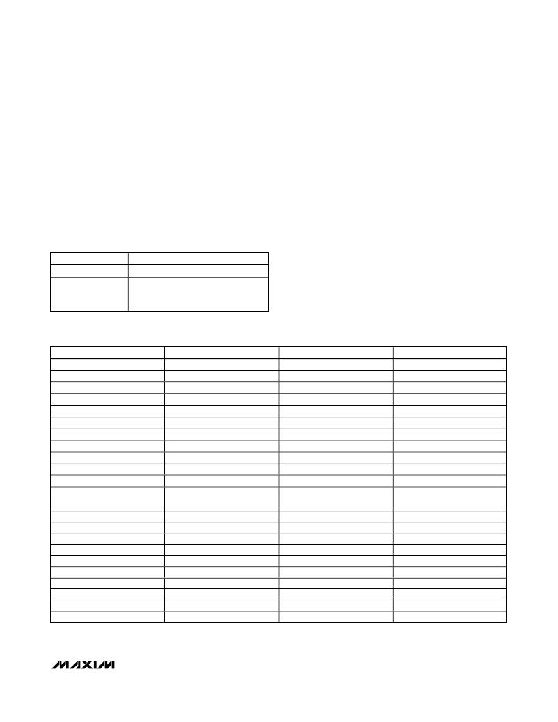
�Table� 2.� Reference� Shunt� Settings� (JU2)�
�SHUNT� POSITION� DESCRIPTION�
�Digital� Data� Headers�
�The� MAX19710–MAX19713� EV� kits� feature� two� 10-bit�
�parallel� data� buses� used� for� full-duplex� operation.� The� two�
�data� buses� are� accessed� on� the� EV� kit� through� header�
�connectors� J2� (Rx� ADC� bus)� and� J3� (Tx� DAC� bus).�
�Digital� Data� Bit� Locations�
�Driver� U2� buffers� the� digital� outputs� of� the� Rx� ADC.� This�
�driver� is� able� to� drive� large� capacitive� loads,� which� may�
�be� present� at� the� logic� analyzer� connection.� The� out-�
�puts� of� the� buffer� are� connected� to� a� 40-pin� header�
�(J2).� The� 20-pin� header� (J3)� is� used� to� connect� to� the�
�digital� input� of� the� Tx� DAC.� See� Table� 3� for� bit� locations�
�on� headers� J2� and� J3.�
�Installed*�
�Not� installed�
�*Default� configuration.�
�Internal� reference� mode.�
�External� reference� mode.�
�Apply� an� external� reference� voltage� to�
�the� REFIN� pad.�
�Configuring� the� Low-Speed� DAC� Buffers�
�The� MAX19710–MAX19713� EV� kits� feature� on-board�
�configurable� buffers.� By� default,� these� buffers� are� config-�
�ured� for� unity� gain.� Measure� the� buffered� voltage� at� the�
�BDAC1,� BDAC2,� and� BDAC3� pads.� Measure� the�
�unbuffered� voltage� at� the� DAC1,� DAC2,� and� DAC3� pads.�
�Table� 3.� Digital� Data� Bit� Locations�
�SIGNAL�
�AD0�
�AD1�
�AD2�
�AD3�
�AD4�
�AD5�
�AD6�
�AD7�
�AD8�
�AD9�
�CLKOUT�
�BDOUT�
�LOCATION�
�J2-37�
�J2-35�
�J2-33�
�J2-31�
�J2-29�
�J2-27�
�J2-25�
�J2-23�
�J2-21�
�J2-19�
�J2-3�
�J2-9�
�TYPE�
�Output�
�Output�
�Output�
�Output�
�Output�
�Output�
�Output�
�Output�
�Output�
�Output�
�Output�
�Output�
�DESCRIPTION�
�Data� Bit� 0� (LSB)�
�Data� Bit� 1�
�Data� Bit� 2�
�Data� Bit� 3�
�Data� Bit� 4�
�Data� Bit� 5�
�Data� Bit� 6�
�Data� Bit� 7�
�Data� Bit� 8�
�Data� Bit� 9� (MSB)�
�Incoming� Clock� Signal�
�Aux-ADC� Digital� Output�
�(requires� R38� short)�
�DA0� J3-19� Input�
�DA1� J3-17� Input�
�DA2� J3-15� Input�
�DA3� J3-13� Input�
�DA4� J3-11� Input�
�DA5� J3-9� Input�
�DA6� J3-7� Input�
�DA7� J3-5� Input�
�DA8� J3-3� Input�
�DA9� J3-1� Input�
�Note:� Pins� 1,� 5,� 7,� 11,� 13,� 15,� 17,� and� 39� of� J2� are� open.� All� other� pins� are� connected� to� OGND.�
�Data� Bit� 0� (LSB)�
�Data� Bit� 1�
�Data� Bit� 2�
�Data� Bit� 3�
�Data� Bit� 4�
�Data� Bit� 5�
�Data� Bit� 6�
�Data� Bit� 7�
�Data� Bit� 8�
�Data� Bit� 9� (MSB)�
�_______________________________________________________________________________________�
�9�
�相关PDF资料 |
PDF描述 |
|---|---|
| 382LX563M025N052 | CAP ALUM 56000UF 25V 20% SNAP |
| CMH322522-330KL | INDUCTOR WIREWOUND 33UH 1210 |
| VI-J5X-EZ-F2 | CONVERTER MOD DC/DC 5.2V 25W |
| GBM24DRYH | CONN EDGECARD 48POS DIP .156 SLD |
| GBC20DRXI-S734 | CONN EDGECARD 40POS DIP .100 SLD |
相关代理商/技术参数 |
参数描述 |
|---|---|
| MAX19711EVKIT+ | 功能描述:数据转换 IC 开发工具 MAX19710/13 Eval Kit RoHS:否 制造商:Texas Instruments 产品:Demonstration Kits 类型:ADC 工具用于评估:ADS130E08 接口类型:SPI 工作电源电压:- 6 V to + 6 V |
| MAX19712ETN | 功能描述:ADC / DAC多通道 RoHS:否 制造商:Texas Instruments 转换速率: 分辨率:8 bit 接口类型:SPI 电压参考: 电源电压-最大:3.6 V 电源电压-最小:2 V 最大工作温度:+ 85 C 安装风格:SMD/SMT 封装 / 箱体:VQFN-40 |
| MAX19712ETN+ | 功能描述:ADC / DAC多通道 22Msps CODEC/AFE Full Duplex RoHS:否 制造商:Texas Instruments 转换速率: 分辨率:8 bit 接口类型:SPI 电压参考: 电源电压-最大:3.6 V 电源电压-最小:2 V 最大工作温度:+ 85 C 安装风格:SMD/SMT 封装 / 箱体:VQFN-40 |
| MAX19712ETN+T | 功能描述:ADC / DAC多通道 22Msps CODEC/AFE Full Duplex RoHS:否 制造商:Texas Instruments 转换速率: 分辨率:8 bit 接口类型:SPI 电压参考: 电源电压-最大:3.6 V 电源电压-最小:2 V 最大工作温度:+ 85 C 安装风格:SMD/SMT 封装 / 箱体:VQFN-40 |
| MAX19712ETN-T | 功能描述:ADC / DAC多通道 RoHS:否 制造商:Texas Instruments 转换速率: 分辨率:8 bit 接口类型:SPI 电压参考: 电源电压-最大:3.6 V 电源电压-最小:2 V 最大工作温度:+ 85 C 安装风格:SMD/SMT 封装 / 箱体:VQFN-40 |
发布紧急采购,3分钟左右您将得到回复。