- 您现在的位置:买卖IC网 > PDF目录383343 > MAX197BCAI (MAXIM INTEGRATED PRODUCTS INC) Multi-Range (【10V, 【5V, +10V, +5V), Single +5V, 12-Bit DAS with 8+4 Bus Interface PDF资料下载
参数资料
| 型号: | MAX197BCAI |
| 厂商: | MAXIM INTEGRATED PRODUCTS INC |
| 元件分类: | 模拟信号调理 |
| 英文描述: | Multi-Range (【10V, 【5V, +10V, +5V), Single +5V, 12-Bit DAS with 8+4 Bus Interface |
| 中文描述: | SPECIALTY ANALOG CIRCUIT, PDSO28 |
| 封装: | 0.209 INCH, SSOP-28 |
| 文件页数: | 11/16页 |
| 文件大小: | 165K |
| 代理商: | MAX197BCAI |
How to Read a Conversion
A standard interrupt signal, INT, is provided to allow the
device to flag the μP when the conversion has ended
and a valid result is available. INT goes low when con-
version is complete and the output data is ready
(Figures 5 and 6). It returns high on the first read cycle
or if a new control byte is written.
Cloc k Modes
The MAX197 operates with either an internal or an
external clock. Control bits (D6, D7) select either inter-
nal or external clock mode. Once the desired clock
mode is selected, changing these bits to program
power-down will not affect the clock mode. In each
mode, internal or external acquisition can be used. At
power-up, external clock mode is selected.
Internal Clock Mode
Select internal clock mode to free the μP from the
burden of running the SAR conversion clock. To select
this mode, write the control byte with D7 = 0 and D6 = 1.
A 100pF capacitor between the CLK pin and ground
sets this frequency to 1.56MHz nominal. Figure 7
shows a linear relationship between the internal clock
period and the value of the external capacitor used.
M
Multi-Range (±10V, ±5V, +10V, +5V ),
S ingle +5V, 12-Bit DAS with 8+4 Bus Interfac e
______________________________________________________________________________________
11
t
CS
t
CSWS
t
WR
t
ACQI
t
CONV
t
DH
t
DS
t
INT1
t
D0
t
D01
t
TR
t
CSHW
t
CSRS
t
CSRH
ACQMOD = "1"
CS
WR
D7–D0
INT
RD
HBEN
DOUT
ACQMOD = "0"
HIGH / LOW
HIGH / LOW
CBYTE
CBYTE
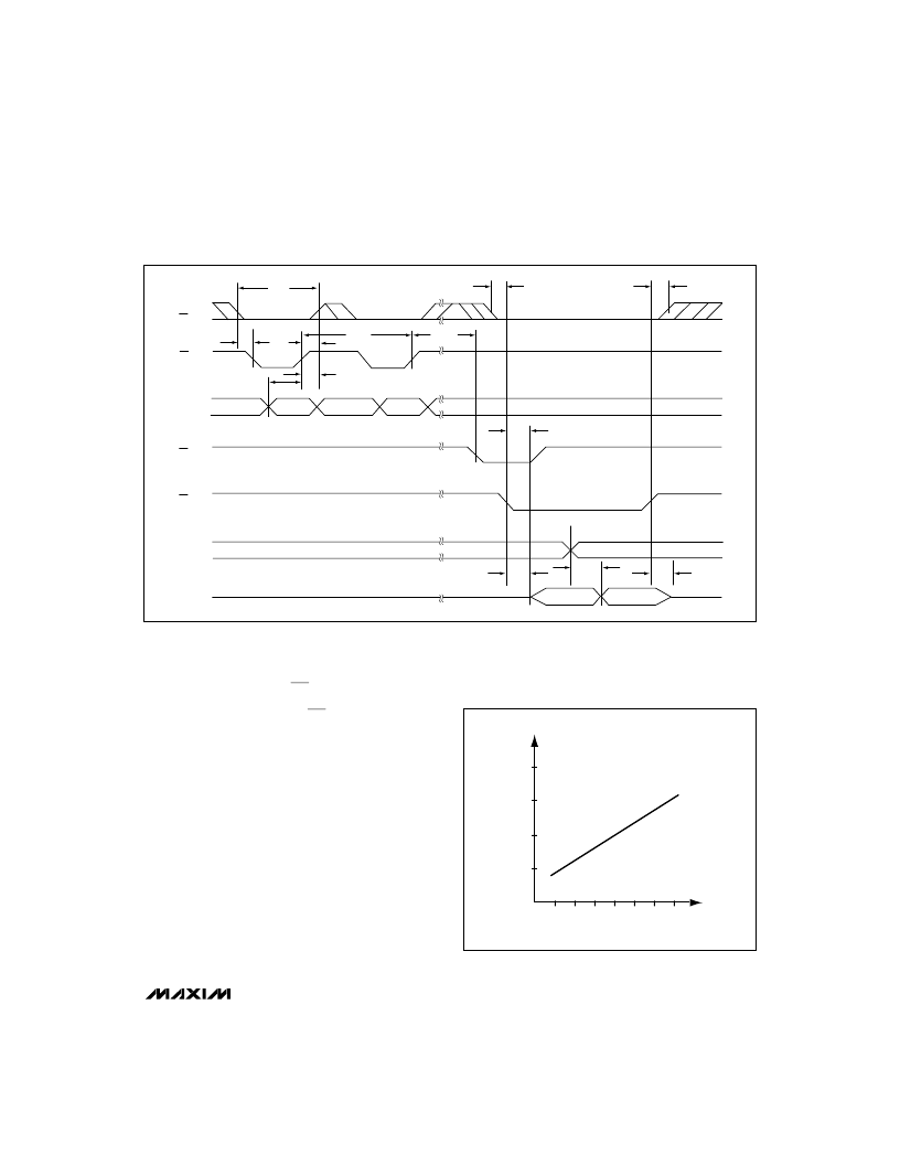
Figure 6. Conversion Timing Using External Acquisition Mode
2000
0
0
50
250
350
500
CLOCK PIN CAPACITANCE (pF)
I
100 150 200
300
1500
1000
Figure 7. Internal Clock Period vs. Clock Pin Capacitance
相关PDF资料 |
PDF描述 |
|---|---|
| MAX197 | Multi-Range Single +5V, 12-Bit DAS with 8+4 Bus Interface(8通道,100ksps,并行,12位A/D转换器) |
| MAX197BCWI | ECONOLINE: RJ & RG - Dual Output from a Single Input Rail - 3kVDC & 4kVDC Isolation - Optional Continuous Short Circuit Protected - Custom Solutions Available - UL94V-0 Package Material - Efficiency to 84% |
| MAX197AENI | Multi-Range (【10V, 【5V, +10V, +5V), Single +5V, 12-Bit DAS with 8+4 Bus Interface |
| MAX197AEWI | Multi-Range (【10V, 【5V, +10V, +5V), Single +5V, 12-Bit DAS with 8+4 Bus Interface |
| MAX197BCNI | Multi-Range (【10V, 【5V, +10V, +5V), Single +5V, 12-Bit DAS with 8+4 Bus Interface |
相关代理商/技术参数 |
参数描述 |
|---|---|
| MAX197BCAI+ | 功能描述:模数转换器 - ADC 12-Bit 8Ch 100ksps 4.18V Precision ADC RoHS:否 制造商:Texas Instruments 通道数量:2 结构:Sigma-Delta 转换速率:125 SPs to 8 KSPs 分辨率:24 bit 输入类型:Differential 信噪比:107 dB 接口类型:SPI 工作电源电压:1.7 V to 3.6 V, 2.7 V to 5.25 V 最大工作温度:+ 85 C 安装风格:SMD/SMT 封装 / 箱体:VQFN-32 |
| MAX197BCAI+T | 功能描述:模数转换器 - ADC 12-Bit 8Ch 100ksps 4.18V Precision ADC RoHS:否 制造商:Texas Instruments 通道数量:2 结构:Sigma-Delta 转换速率:125 SPs to 8 KSPs 分辨率:24 bit 输入类型:Differential 信噪比:107 dB 接口类型:SPI 工作电源电压:1.7 V to 3.6 V, 2.7 V to 5.25 V 最大工作温度:+ 85 C 安装风格:SMD/SMT 封装 / 箱体:VQFN-32 |
| MAX197BCAI-T | 功能描述:模数转换器 - ADC RoHS:否 制造商:Texas Instruments 通道数量:2 结构:Sigma-Delta 转换速率:125 SPs to 8 KSPs 分辨率:24 bit 输入类型:Differential 信噪比:107 dB 接口类型:SPI 工作电源电压:1.7 V to 3.6 V, 2.7 V to 5.25 V 最大工作温度:+ 85 C 安装风格:SMD/SMT 封装 / 箱体:VQFN-32 |
| MAX197BCNI | 功能描述:模数转换器 - ADC Integrated Circuits (ICs) RoHS:否 制造商:Texas Instruments 通道数量:2 结构:Sigma-Delta 转换速率:125 SPs to 8 KSPs 分辨率:24 bit 输入类型:Differential 信噪比:107 dB 接口类型:SPI 工作电源电压:1.7 V to 3.6 V, 2.7 V to 5.25 V 最大工作温度:+ 85 C 安装风格:SMD/SMT 封装 / 箱体:VQFN-32 |
| MAX197BCNI+ | 功能描述:模数转换器 - ADC 12-Bit 8Ch 100ksps 4.18V Precision ADC RoHS:否 制造商:Texas Instruments 通道数量:2 结构:Sigma-Delta 转换速率:125 SPs to 8 KSPs 分辨率:24 bit 输入类型:Differential 信噪比:107 dB 接口类型:SPI 工作电源电压:1.7 V to 3.6 V, 2.7 V to 5.25 V 最大工作温度:+ 85 C 安装风格:SMD/SMT 封装 / 箱体:VQFN-32 |
发布紧急采购,3分钟左右您将得到回复。