- 您现在的位置:买卖IC网 > PDF目录383343 > MAX197BMYI (MAXIM INTEGRATED PRODUCTS INC) Multi-Range (【10V, 【5V, +10V, +5V), Single +5V, 12-Bit DAS with 8+4 Bus Interface PDF资料下载
参数资料
| 型号: | MAX197BMYI |
| 厂商: | MAXIM INTEGRATED PRODUCTS INC |
| 元件分类: | 模拟信号调理 |
| 英文描述: | Multi-Range (【10V, 【5V, +10V, +5V), Single +5V, 12-Bit DAS with 8+4 Bus Interface |
| 中文描述: | SPECIALTY ANALOG CIRCUIT, CDIP28 |
| 封装: | SIDE BRAZED, CERAMIC, DIP-28 |
| 文件页数: | 9/16页 |
| 文件大小: | 165K |
| 代理商: | MAX197BMYI |
The input channels are overvoltage protected to
±16.5V. This protection is active even if the device is in
power-down mode.
Even with V
DD
= 0V, the input resistive network provides
current-limiting that adequately protects the device.
Digital Interfac e
Input data (control byte) and output data are multiplexed
on a three-state parallel interface. This parallel I/O can
easily be interfaced with a μP. CS, WR, and RD control
the write and read operations. CS is the standard chip-
select signal, which enables a μP to address the MAX197
as an I/O port. When high, it disables the WR and RD
inputs and forces the interface into a high-Z state.
Input Format
The control byte is latched into the device, on pins
D7–D0, during a write cycle. Table 2 shows the control-
byte format.
Output Data Format
The output data format is binary in unipolar mode and
twos-complement binary in bipolar mode. When read-
ing the output data, CS, and RD must be low. When
HBEN is low, the lower eight bits are read. When HBEN
is high, the upper four MSBs are available and the out-
put data bits D4–D7 are either set low (in unipolar
mode) or set to the value of the MSB (in bipolar mode)
(Table 6).
M
Multi-Range (±10V, ±5V, +10V, +5V ),
S ingle +5V, 12-Bit DAS with 8+4 Bus Interfac e
_______________________________________________________________________________________
9
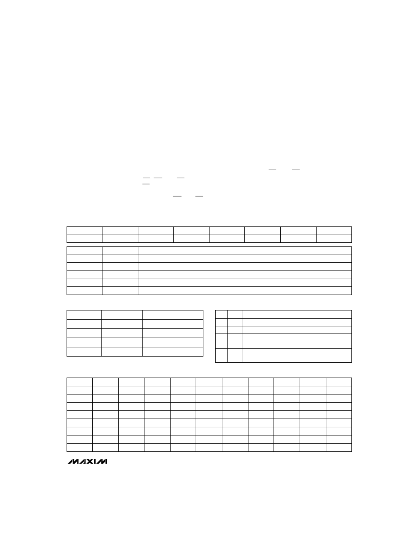
Table 2. Control-Byte Format
D7 (MSB)
PD1
D6
PD0
D5
D4
RNG
D3
BIP
D2
A2
D1
A1
D0 (LSB)
A0
ACQMOD
Table 4. Clock and Power-Down Selection
PD1 PD0
0
0
DEVICE MODE
0
1
Normal Operation / External Clock Mode
Normal Operation / Internal Clock Mode
1
0
Standby Power-Down (STBYPD); clock mode
is unaffected
1
1
Full Power-Down (FULLPD); clock mode is
unaffected
Table 3. Range and Polarity Selection
BIP
RNG
INPUT RANGE (V)
0
0
0 to 5
0
1
0 to 10
1
0
±5
1
1
±10
Table 5. Channel Selection
A2
A1
A0
CH0
CH1
CH2
CH3
CH4
CH5
CH6
CH7
0
0
0
0
0
1
0
1
0
0
1
1
1
0
0
1
0
1
1
1
0
1
1
1
BIT
NAME
DESCRIPTION
7, 6
PD1, PD0
These two bits select the clock and power-down modes (Table 4).
5
ACQMOD
0 = internally controlled acquisition (6 clock cycles), 1 = externally controlled acquisition
4
RNG
Selects the full-scale voltage magnitude at the input (Table 3).
3
BIP
Selects unipolar or bipolar conversion mode (Table 3).
These are address bits for the input mux to select the “on” channel (Table 5).
2, 1, 0
A2, A1, A0
相关PDF资料 |
PDF描述 |
|---|---|
| MAX1980 | Quick-PWM Slave Controller with Driver Disable for Multiphase DC-DC Converter |
| MAX1980ETP | Quick-PWM Slave Controller with Driver Disable for Multiphase DC-DC Converter |
| MAX1982 | Low-Voltage, Low-Dropout Linear Regulators with External Bias Supply |
| MAX1982-MAX1983 | EPS300 3/4 CR 48 IN 5700750CR |
| MAX1982EUT-T | Low-Voltage, Low-Dropout Linear Regulators with External Bias Supply |
相关代理商/技术参数 |
参数描述 |
|---|---|
| MAX197EVC16-DIP | 功能描述:模数转换器 - ADC Programmers, Development Systems RoHS:否 制造商:Texas Instruments 通道数量:2 结构:Sigma-Delta 转换速率:125 SPs to 8 KSPs 分辨率:24 bit 输入类型:Differential 信噪比:107 dB 接口类型:SPI 工作电源电压:1.7 V to 3.6 V, 2.7 V to 5.25 V 最大工作温度:+ 85 C 安装风格:SMD/SMT 封装 / 箱体:VQFN-32 |
| MAX197EVC32-DIP | 功能描述:模数转换器 - ADC Programmers, Development Systems RoHS:否 制造商:Texas Instruments 通道数量:2 结构:Sigma-Delta 转换速率:125 SPs to 8 KSPs 分辨率:24 bit 输入类型:Differential 信噪比:107 dB 接口类型:SPI 工作电源电压:1.7 V to 3.6 V, 2.7 V to 5.25 V 最大工作温度:+ 85 C 安装风格:SMD/SMT 封装 / 箱体:VQFN-32 |
| MAX197EVKIT-DIP | 功能描述:数据转换 IC 开发工具 Programmers, Development Systems RoHS:否 制造商:Texas Instruments 产品:Demonstration Kits 类型:ADC 工具用于评估:ADS130E08 接口类型:SPI 工作电源电压:- 6 V to + 6 V |
| MAX1980EGP | 功能描述:DC/DC 开关控制器 RoHS:否 制造商:Texas Instruments 输入电压:6 V to 100 V 开关频率: 输出电压:1.215 V to 80 V 输出电流:3.5 A 输出端数量:1 最大工作温度:+ 125 C 安装风格: 封装 / 箱体:CPAK |
| MAX1980EGP-T | 功能描述:DC/DC 开关控制器 RoHS:否 制造商:Texas Instruments 输入电压:6 V to 100 V 开关频率: 输出电压:1.215 V to 80 V 输出电流:3.5 A 输出端数量:1 最大工作温度:+ 125 C 安装风格: 封装 / 箱体:CPAK |
发布紧急采购,3分钟左右您将得到回复。