- 您现在的位置:买卖IC网 > PDF目录383344 > MAX1984 (Maxim Integrated Products, Inc.) Ultra-High-Efficiency White LED Drivers PDF资料下载
参数资料
| 型号: | MAX1984 |
| 厂商: | Maxim Integrated Products, Inc. |
| 元件分类: | LED驱动器 |
| 英文描述: | Ultra-High-Efficiency White LED Drivers |
| 中文描述: | 超高效率白光LED驱动器 |
| 文件页数: | 2/17页 |
| 文件大小: | 333K |
| 代理商: | MAX1984 |
M
Ultra-High-Efficiency White
LED Drivers
2
_______________________________________________________________________________________
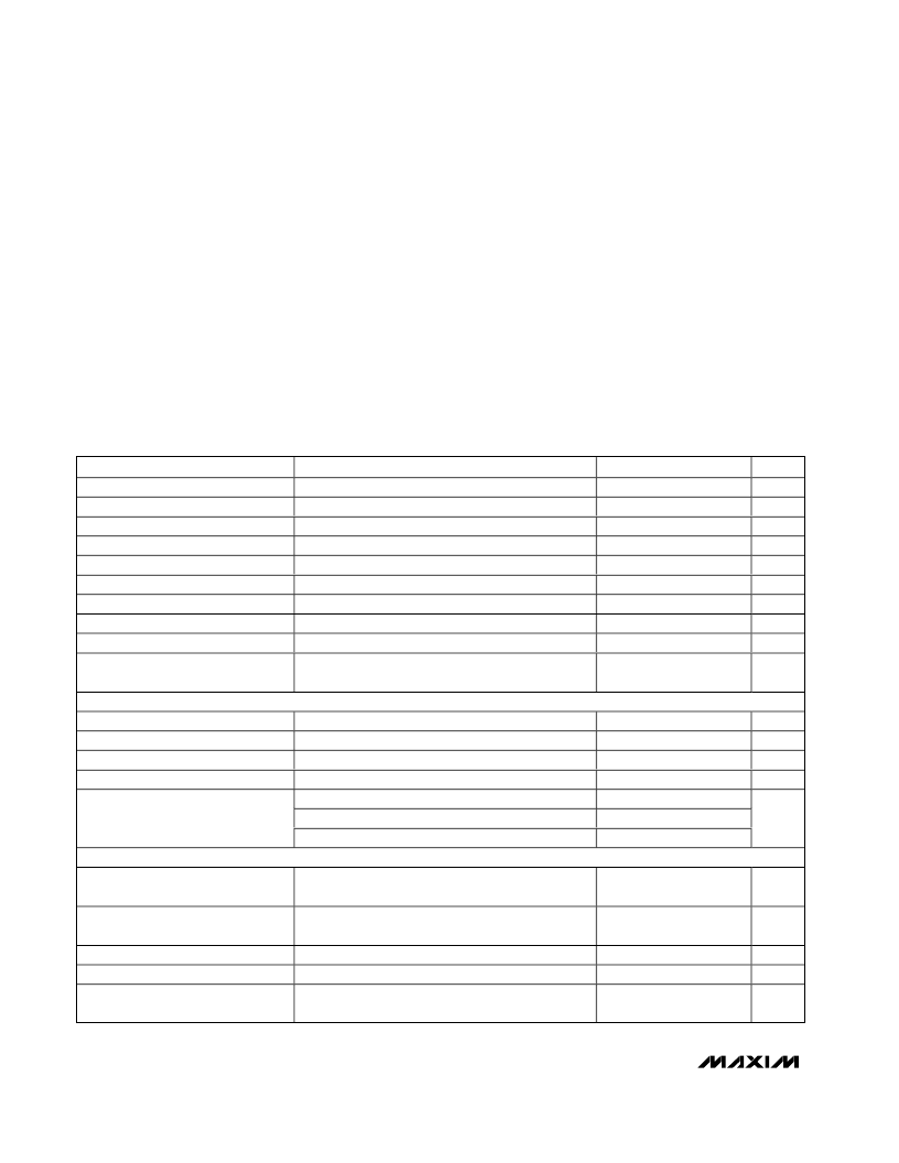
ABSOLUTE MAXIMUM RATINGS
OUT, IN, BITA, BITB, BITC, LD1, LD2, LD3, LD4,
LD5, LD6, LD7, LD8 to GND................................-0.3V to +6V
LDG to GND........................................................................±0.3V
LX to GND ................................................-0.3V to (V
OUT
+ 0.3V)
SETI, REF, MODE, SEL to GND...................-0.3V to (V
IN
+ 0.3V)
Continuous Power Dissipation (T
A
= +70°C)
16-Pin Thin QFN (derate 16.9mW/°C above +70°C) ...1349mW
20-Pin Thin QFN (derate 16.9mW/°C above +70°C) ...1349mW
ELECTRICAL CHARACTERISTICS
(Circuit of Figure 1; V
IN
= 3.3V, SETI = BITA = BITB = BITC = SEL = IN, MODE = GND, C
OUT
= 4.7μF, C
REF
= 0.22μF,
T
A
= 0°C to +85°C
,
unless otherwise noted. Typical values are at T
A
= +25°C.)
Stresses beyond those listed under “Absolute Maximum Ratings” may cause permanent damage to the device. These are stress ratings only, and functional
operation of the device at these or any other conditions beyond those indicated in the operational sections of the specifications is not implied. Exposure to
absolute maximum rating conditions for extended periods may affect device reliability.
Operating Temperature Range ...........................-40°C to +85°C
Junction Temperature......................................................+150°C
Storage Temperature Range.............................-65°C to +150°C
Lead Temperature (soldering, 10s).................................+300°C
PARAMETER
CONDITIONS
MIN
2.7
2.2
TYP
MAX
5.5
2.6
600
1
1.270
5
15
1.2
UNITS
V
V
μA
μA
V
mV
mV
MHz
%
IN Supply Range
IN Undervoltage Lockout Threshold
IN Quiescent Current
IN Shutdown Current
REF Output Voltage
REF Line Regulation
REF Load Regulation
Oscillator Frequency
Oscillator Maximum Duty Cycle
50mV typical hysteresis
BITA = BITB = BITC = IN, LD1 to LD8 = GND
BITA = BITB = BITC = GND
I
REF
= 0
2.7V < V
IN
< 5.5V
-1μA < I
REF
< +50μA
2.4
400
0.1
1.250
0.2
5
1
85
1.230
0.8
OUT Overvoltage Protection (OVP)
Threshold
V
LD1
to V
LD8
= 50mV, OUT rising, 100mV typical
hysteresis
5.1
5.3
5.5
V
INTERNAL MOSFET SWITCHES
N-Channel MOSFET On-Resistance
N-Channel MOSFET Leakage Current
P-Channel MOSFET On-Resistance
P-Channel MOSFET Leakage Current
I
LX
= 200mA
V
LX
= 5.5V, BITA = BITB = BITC = GND
I
LX
= 200mA
LX = GND, V
OUT
= 5.5V, BITA = BITB = BITC = GND
MAX1984
MAX1985
MAX1986
0.4
0.1
0.5
0.1
0.65
0.52
0.39
0.8
1
1
1
0.81
0.65
0.52
μA
μA
0.50
0.40
0.30
N-Channel MOSFET Current Limit
A
CONTROL INPUTS
BITA, BITB, BITC Input Logic Low
Level
BITA, BITB, BITC Input Logic High
Level
MODE Input Logic Low Level
MODE Input Logic High Level
MODE, BITA, BITB, BITC Input Bias
Current
2.7V < V
IN
< 5.5V
0.4
V
2.7V < V
IN
< 5.5V
1.6
V
2.7V < V
IN
< 5.5V
2.7V < V
IN
< 5.5V
0.4
V
V
V
IN
- 0.4
2.7V < V
IN
< 5.5V
0.01
1
μA
相关PDF资料 |
PDF描述 |
|---|---|
| MAX1984ETP | Ultra-High-Efficiency White LED Drivers |
| MAX1985ETP | Ultra-High-Efficiency White LED Drivers |
| MAX1986ETE | Ultra-High-Efficiency White LED Drivers |
| MAX1994ETM | Dual Step-Down Controllers Plus Linear- Regulator Controller for Notebook Computers |
| MAX1816 | Replaced by TMS320VC5506 : Digital Signal Processors 144-LQFP |
相关代理商/技术参数 |
参数描述 |
|---|---|
| MAX1984ETP | 功能描述:LED照明驱动器 RoHS:否 制造商:STMicroelectronics 输入电压:11.5 V to 23 V 工作频率: 最大电源电流:1.7 mA 输出电流: 最大工作温度: 安装风格:SMD/SMT 封装 / 箱体:SO-16N |
| MAX1984ETP+ | 功能描述:LED照明驱动器 High-Efficiency White LED Driver RoHS:否 制造商:STMicroelectronics 输入电压:11.5 V to 23 V 工作频率: 最大电源电流:1.7 mA 输出电流: 最大工作温度: 安装风格:SMD/SMT 封装 / 箱体:SO-16N |
| MAX1984ETP+T | 功能描述:LED照明驱动器 High-Efficiency White LED Driver RoHS:否 制造商:STMicroelectronics 输入电压:11.5 V to 23 V 工作频率: 最大电源电流:1.7 mA 输出电流: 最大工作温度: 安装风格:SMD/SMT 封装 / 箱体:SO-16N |
| MAX1984ETP-T | 功能描述:LED照明驱动器 RoHS:否 制造商:STMicroelectronics 输入电压:11.5 V to 23 V 工作频率: 最大电源电流:1.7 mA 输出电流: 最大工作温度: 安装风格:SMD/SMT 封装 / 箱体:SO-16N |
| MAX1985ETP | 功能描述:LED照明驱动器 RoHS:否 制造商:STMicroelectronics 输入电压:11.5 V to 23 V 工作频率: 最大电源电流:1.7 mA 输出电流: 最大工作温度: 安装风格:SMD/SMT 封装 / 箱体:SO-16N |
发布紧急采购,3分钟左右您将得到回复。