- 您现在的位置:买卖IC网 > Datasheet目录471 > MAX19999ETX+T (Maxim Integrated)IC DOWNCONVERTER 2CH 36TQFN Datasheet资料下载
参数资料
| 型号: | MAX19999ETX+T |
| 厂商: | Maxim Integrated |
| 文件页数: | 2/19页 |
| 文件大小: | 0K |
| 描述: | IC DOWNCONVERTER 2CH 36TQFN |
| 产品培训模块: | Lead (SnPb) Finish for COTS Obsolescence Mitigation Program |
| 标准包装: | 2,500 |
| RF 型: | LTE,WiMAX,WLL |
| 频率: | 3GHz ~ 4GHz |
| 混频器数目: | 1 |
| 增益: | 8.3dB |
| 噪音数据: | 10.5dB |
| 次要属性: | 降频变频器 |
| 电流 - 电源: | 279mA,420mA |
| 电源电压: | 3 V ~ 3.6 V,4.75 V ~ 5.25 V |
| 包装: | 带卷 (TR) |
| 封装/外壳: | 36-WFQFN 裸露焊盘 |
| 供应商设备封装: | 36-TQFN 裸露焊盘(6x6) |
�� �
�
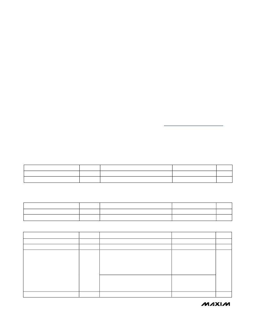
�Dual,� SiGe� High-Linearity,� 3000MHz� to�
�4000MHz� Downconversion� Mixer� with� LO� Buffer�
�ABSOLUTE� MAXIMUM� RATINGS�
�V� CC� to� GND� ...........................................................-0.3V� to� +5.5V�
�RF_,� LO� to� GND.....................................................-0.3V� to� +0.3V�
�IFM_,� IFD_,� IFM_SET,� IFD_SET,� LO_ADJ_M,�
�LO_ADJ_D� to� GND.................................-0.3V� to� (V� CC� +� 0.3V)�
�RF_,� LO� Input� Power� ......................................................+15dBm�
�RF_,� LO� Current� (RF� and� LO� are� DC� shorted� to� GND�
�through� balun).................................................................50mA�
�θ� JA� (Notes� 2,� 3)..............................................................+38°C/W�
�θ� JC� (Note� 3).....................................................................7.4°C/W�
�Operating� Case� Temperature� Range�
�(Note� 4)� ...................................................T� C� =� -40°C� to� +85°C�
�Junction� Temperature� ......................................................+150°C�
�Storage� Temperature� Range� .............................-65°C� to� +150°C�
�Lead� Temperature� (soldering,� 10s)� .................................+300°C�
�Continuous� Power� Dissipation� (Note� 1)� ..............................8.7W�
�Note� 1:� Based� on� junction� temperature� T� J� =� T� C� +� (� θ� JC� x� V� CC� x� I� CC� ).� This� formula� can� be� used� when� the� temperature� of� the� exposed�
�pad� is� known� while� the� device� is� soldered� down� to� a� PCB.� See� the� Applications� Information� section� for� details.� The� junction�
�temperature� must� not� exceed� +150°C.�
�Note� 2:� Junction� temperature� T� J� =� T� A� +� (� θ� JA� x� V� CC� x� I� CC� ).� This� formula� can� be� used� when� the� ambient� temperature� of� the� PCB� is�
�known.� The� junction� temperature� must� not� exceed� +150°C.�
�Note� 3:� Package� thermal� resistances� were� obtained� using� the� method� described� in� JEDEC� specification� JESD51-7,� using� a� four-�
�layer� board.� For� detailed� information� on� package� thermal� considerations,� refer� to� www.maxim-ic.com/thermal-tutorial� .�
�Note� 4:� T� C� is� the� temperature� on� the� exposed� pad� of� the� package.� TA� is� the� ambient� temperature� of� the� device� and� PCB.�
�Stresses� beyond� those� listed� under� “Absolute� Maximum� Ratings”� may� cause� permanent� damage� to� the� device.� These� are� stress� ratings� only,� and� functional�
�operation� of� the� device� at� these� or� any� other� conditions� beyond� those� indicated� in� the� operational� sections� of� the� specifications� is� not� implied.� Exposure� to�
�absolute� maximum� rating� conditions� for� extended� periods� may� affect� device� reliability.�
�+5.0V� SUPPLY� DC� ELECTRICAL� CHARACTERISTICS�
�(Typical� Application� Circuit,� no� input� RF� or� LO� signals� applied,� V� CC� =� +4.75V� to� +5.25V,� T� C� =� -40°C� to� +85°C.� Typical� values� are� at�
�V� CC� =� +5.0V,� T� C� =� +25°C,� unless� otherwise� noted.� R1� =� R4� =� 750� Ω� ,� R2� =� R5� =� 698� Ω� .)�
�PARAMETER�
�SYMBOL�
�CONDITIONS�
�MIN�
�TYP�
�MAX�
�UNITS�
�Supply� Voltage�
�Supply� Current�
�V� CC�
�I� CC�
�Total� supply� current�
�4.75�
�5�
�388�
�5.25�
�420�
�V�
�mA�
�+3.3V� SUPPLY� DC� ELECTRICAL� CHARACTERISTICS�
�(� Typical� Application� Circuit� ,� no� input� RF� or� LO� signals� applied,� T� C� =� -40°C� to� +85°C.� Typical� values� are� at�
�V� CC� =� +3.3V,� T� C� =� +25°C,� unless� otherwise� noted.� R1� =� R4� =� 1.1k� Ω� ;� R2� =� R5� =� 845� Ω� .)� (Note� 5)�
�PARAMETER�
�Supply� Voltage�
�Supply� Current�
�SYMBOL�
�V� CC�
�I� CC�
�CONDITIONS�
�(Note� 6)�
�Total� supply� current�
�MIN�
�3�
�TYP�
�3.3�
�279�
�MAX�
�3.6�
�UNITS�
�V�
�mA�
�RECOMMENDED� AC� OPERATING� CONDITIONS�
�PARAMETER�
�RF� Frequency�
�LO� Frequency�
�SYMBOL�
�f� RF�
�f� LO�
�(Notes� 5,� 7)�
�(Notes� 5,� 7)�
�CONDITIONS�
�MIN�
�3000�
�2650�
�TYP�
�MAX�
�4000�
�3700�
�UNITS�
�MHz�
�MHz�
�Using� Mini-Circuits� TC4-1W-17� 4:1�
�transformer� as� defined� in� the� Typical�
�Application� Circuit� ,� IF� matching�
�components� affect� the� IF� frequency� range�
�100�
�500�
�IF� Frequency�
�f� IF�
�(Notes� 5,� 7)�
�MHz�
�Using� alternative� Mini-Circuits� TC4-1W-7A�
�4:1� transformer,� IF� matching� components�
�affect� the� IF� frequency� range� (Notes� 5,� 7)�
�50�
�250�
�LO� Drive� Level�
�P� LO�
�(Note� 7)�
�-3�
�+3�
�dBm�
�2�
�_______________________________________________________________________________________�
�相关PDF资料 |
PDF描述 |
|---|---|
| MAX2009ETI+T | IC RF PREDISTORT ADJ 28-TQFN |
| MAX2010ETI+T | IC RF PREDISTORT ADJ 28-TQFN |
| MAX2014ETA+T | IC DETECT/CNTRL LOG 8-TDFN |
| MAX2015EUA+T | IC DETECT/CNTRL LOG 8-UMAX |
| MAX2015EVKIT | EVAL KIT FOR MAX2015 |
相关代理商/技术参数 |
参数描述 |
|---|---|
| MAX1999EEI | 功能描述:DC/DC 开关控制器 RoHS:否 制造商:Texas Instruments 输入电压:6 V to 100 V 开关频率: 输出电压:1.215 V to 80 V 输出电流:3.5 A 输出端数量:1 最大工作温度:+ 125 C 安装风格: 封装 / 箱体:CPAK |
| MAX1999EEI+ | 功能描述:DC/DC 开关控制器 Quad Out Main Power Supply Controller RoHS:否 制造商:Texas Instruments 输入电压:6 V to 100 V 开关频率: 输出电压:1.215 V to 80 V 输出电流:3.5 A 输出端数量:1 最大工作温度:+ 125 C 安装风格: 封装 / 箱体:CPAK |
| MAX1999EEI+T | 功能描述:DC/DC 开关控制器 Quad Out Main Power Supply Controller RoHS:否 制造商:Texas Instruments 输入电压:6 V to 100 V 开关频率: 输出电压:1.215 V to 80 V 输出电流:3.5 A 输出端数量:1 最大工作温度:+ 125 C 安装风格: 封装 / 箱体:CPAK |
| MAX1999EEI-T | 功能描述:DC/DC 开关控制器 RoHS:否 制造商:Texas Instruments 输入电压:6 V to 100 V 开关频率: 输出电压:1.215 V to 80 V 输出电流:3.5 A 输出端数量:1 最大工作温度:+ 125 C 安装风格: 封装 / 箱体:CPAK |
| MAX1999EVKIT | 功能描述:DC/DC 开关控制器 Evaluation Kit for the MAX1777 MAX1977 MAX1999 RoHS:否 制造商:Texas Instruments 输入电压:6 V to 100 V 开关频率: 输出电压:1.215 V to 80 V 输出电流:3.5 A 输出端数量:1 最大工作温度:+ 125 C 安装风格: 封装 / 箱体:CPAK |
发布紧急采购,3分钟左右您将得到回复。