- 您现在的位置:买卖IC网 > PDF目录383344 > MAX199BENI (MAXIM INTEGRATED PRODUCTS INC) Multi-Range (【4V, 【2V, +4V, +2V), +5V Supply, 12-Bit DAS with 8+4 Bus Interface PDF资料下载
参数资料
| 型号: | MAX199BENI |
| 厂商: | MAXIM INTEGRATED PRODUCTS INC |
| 元件分类: | 模拟信号调理 |
| 英文描述: | Multi-Range (【4V, 【2V, +4V, +2V), +5V Supply, 12-Bit DAS with 8+4 Bus Interface |
| 中文描述: | SPECIALTY ANALOG CIRCUIT, PDIP28 |
| 封装: | 0.300 INCH, PLASTIC, DIP-28 |
| 文件页数: | 7/16页 |
| 文件大小: | 165K |
| 代理商: | MAX199BENI |
M
Multi-Range (±4V, ±2V, +4V, +2V ),
+5V S upply, 12-Bit DAS with 8+4 Bus Interfac e
_______________________________________________________________________________________
7
______________________________________________________________Pin Desc ription
Digital Ground
DGND
28
+5V Supply. Bypass with 0.1μF capacitor to AGND.
V
DD
27
INT goes low when conversion is complete and output data is ready.
INT
24
Bandgap Voltage-Reference Output / External Adjust Pin. Bypass with a 0.01μF capacitor to AGND.
Connect to V
DD
when using an external reference at the REF pin.
REFADJ
25
Reference Buffer Output / ADC Reference Input. In internal reference mode, the reference buffer provides a
4.096V nominal output, externally adjustable at REFADJ . In external reference mode, disable the internal
buffer by pulling REFADJ to V
DD
.
REF
26
Three-State Digital I/O. D2 output (HBEN = low), D10 output (HBEN = high).
Three-State Digital I/O. D1 output (HBEN = low), D9 output (HBEN = high).
Three-State Digital I/O. D0 output (HBEN = low), D8 output (HBEN = high). D0 = LSB.
Analog Ground
Analog Input Channels
D2/D10
D1/D9
D0/D8
AGND
CH0–CH7
12
13
14
15
16–23
Used to multiplex the 12-bit conversion result. When high, the 4 MSBs are multiplexed on the data bus;
when low, the 8 LSBs are available on the bus.
HBEN
5
Shutdown. Puts the device into full power-down (FULLPD) mode when pulled low.
Three-State Digital I/O
Three-State Digital I/O. D3 output (HBEN = low), D11 output (HBEN = high).
SHDN
D7–D4
D3/D11
6
7–10
11
When CS is low, a falling edge on RD will enable a read operation on the data bus.
RD
4
When CS is low, in the internal acquisition mode, a rising edge on WRlatches in configuration data and starts an
acquisition plus a conversion cycle. When CS is low, in the external acquisition mode, the first rising edge on
WR starts an acquisition and a second rising edge on WR ends acquisition and starts a conversion cycle.
WR
3
PIN
Chip Select, active low.
CS
2
Clock Input. In external clock mode, drive CLK with a TTL/CMOS compatible clock. In internal clock mode,
place a capacitor (C
CLK
) from this pin to ground to set the internal clock frequency; f
CLK
= 1.56MHz typical
with C
CLK
= 100pF.
CLK
1
FUNCTION
NAME
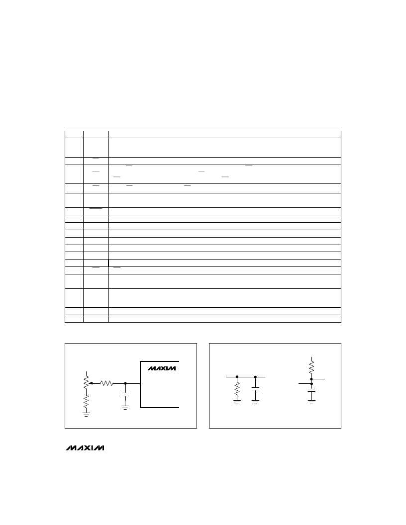
100k
510k
24k
REFADJ
+5V
0.01
μ
F
MAX199
Figure 1. Reference-Adjust Circuit
3k
3k
D
OUT
D
OUT
+5V
a)
High-Z to V
OH
and V
OL
to V
OH
b)
High-Z to V
OL
and V
OH
to V
OL
C
LOAD
C
LOAD
Figure 2. Load Circuits for Enable Time
相关PDF资料 |
PDF描述 |
|---|---|
| MAX199BCWI | Multi-Range (【4V, 【2V, +4V, +2V), +5V Supply, 12-Bit DAS with 8+4 Bus Interface |
| MAX199BCNI | Multi-Range (【4V, 【2V, +4V, +2V), +5V Supply, 12-Bit DAS with 8+4 Bus Interface |
| MAX199BEWI | Fixed-Point Digital Signal Processor 532-FCBGA |
| MAX199ACNI | Multi-Range (【4V, 【2V, +4V, +2V), +5V Supply, 12-Bit DAS with 8+4 Bus Interface |
| MAX199ACWI | Multi-Range (【4V, 【2V, +4V, +2V), +5V Supply, 12-Bit DAS with 8+4 Bus Interface |
相关代理商/技术参数 |
参数描述 |
|---|---|
| MAX199BENI+ | 功能描述:模数转换器 - ADC 12Bit 8Ch 100ksps 4.18V Precision ADC RoHS:否 制造商:Texas Instruments 通道数量:2 结构:Sigma-Delta 转换速率:125 SPs to 8 KSPs 分辨率:24 bit 输入类型:Differential 信噪比:107 dB 接口类型:SPI 工作电源电压:1.7 V to 3.6 V, 2.7 V to 5.25 V 最大工作温度:+ 85 C 安装风格:SMD/SMT 封装 / 箱体:VQFN-32 |
| MAX199BEWI | 功能描述:模数转换器 - ADC RoHS:否 制造商:Texas Instruments 通道数量:2 结构:Sigma-Delta 转换速率:125 SPs to 8 KSPs 分辨率:24 bit 输入类型:Differential 信噪比:107 dB 接口类型:SPI 工作电源电压:1.7 V to 3.6 V, 2.7 V to 5.25 V 最大工作温度:+ 85 C 安装风格:SMD/SMT 封装 / 箱体:VQFN-32 |
| MAX199BEWI+ | 功能描述:模数转换器 - ADC 12Bit 8Ch 100ksps 4.18V Precision ADC RoHS:否 制造商:Texas Instruments 通道数量:2 结构:Sigma-Delta 转换速率:125 SPs to 8 KSPs 分辨率:24 bit 输入类型:Differential 信噪比:107 dB 接口类型:SPI 工作电源电压:1.7 V to 3.6 V, 2.7 V to 5.25 V 最大工作温度:+ 85 C 安装风格:SMD/SMT 封装 / 箱体:VQFN-32 |
| MAX199BEWI+T | 功能描述:模数转换器 - ADC 12Bit 8Ch 100ksps 4.18V Precision ADC RoHS:否 制造商:Texas Instruments 通道数量:2 结构:Sigma-Delta 转换速率:125 SPs to 8 KSPs 分辨率:24 bit 输入类型:Differential 信噪比:107 dB 接口类型:SPI 工作电源电压:1.7 V to 3.6 V, 2.7 V to 5.25 V 最大工作温度:+ 85 C 安装风格:SMD/SMT 封装 / 箱体:VQFN-32 |
| MAX199BEWI-T | 功能描述:模数转换器 - ADC RoHS:否 制造商:Texas Instruments 通道数量:2 结构:Sigma-Delta 转换速率:125 SPs to 8 KSPs 分辨率:24 bit 输入类型:Differential 信噪比:107 dB 接口类型:SPI 工作电源电压:1.7 V to 3.6 V, 2.7 V to 5.25 V 最大工作温度:+ 85 C 安装风格:SMD/SMT 封装 / 箱体:VQFN-32 |
发布紧急采购,3分钟左右您将得到回复。