- 您现在的位置:买卖IC网 > PDF目录383344 > MAX199BMYI (MAXIM INTEGRATED PRODUCTS INC) Multi-Range (【4V, 【2V, +4V, +2V), +5V Supply, 12-Bit DAS with 8+4 Bus Interface PDF资料下载
参数资料
| 型号: | MAX199BMYI |
| 厂商: | MAXIM INTEGRATED PRODUCTS INC |
| 元件分类: | 模拟信号调理 |
| 英文描述: | Multi-Range (【4V, 【2V, +4V, +2V), +5V Supply, 12-Bit DAS with 8+4 Bus Interface |
| 中文描述: | SPECIALTY ANALOG CIRCUIT, CDIP28 |
| 封装: | 0.600 INCH, SIDE BRAZED, CERAMIC, DIP-28 |
| 文件页数: | 7/16页 |
| 文件大小: | 165K |
| 代理商: | MAX199BMYI |
M
Multi-Range (±4V, ±2V, +4V, +2V ),
+5V S upply, 12-Bit DAS with 8+4 Bus Interfac e
_______________________________________________________________________________________
7
______________________________________________________________Pin Desc ription
Digital Ground
DGND
28
+5V Supply. Bypass with 0.1μF capacitor to AGND.
V
DD
27
INT goes low when conversion is complete and output data is ready.
INT
24
Bandgap Voltage-Reference Output / External Adjust Pin. Bypass with a 0.01μF capacitor to AGND.
Connect to V
DD
when using an external reference at the REF pin.
REFADJ
25
Reference Buffer Output / ADC Reference Input. In internal reference mode, the reference buffer provides a
4.096V nominal output, externally adjustable at REFADJ . In external reference mode, disable the internal
buffer by pulling REFADJ to V
DD
.
REF
26
Three-State Digital I/O. D2 output (HBEN = low), D10 output (HBEN = high).
Three-State Digital I/O. D1 output (HBEN = low), D9 output (HBEN = high).
Three-State Digital I/O. D0 output (HBEN = low), D8 output (HBEN = high). D0 = LSB.
Analog Ground
Analog Input Channels
D2/D10
D1/D9
D0/D8
AGND
CH0–CH7
12
13
14
15
16–23
Used to multiplex the 12-bit conversion result. When high, the 4 MSBs are multiplexed on the data bus;
when low, the 8 LSBs are available on the bus.
HBEN
5
Shutdown. Puts the device into full power-down (FULLPD) mode when pulled low.
Three-State Digital I/O
Three-State Digital I/O. D3 output (HBEN = low), D11 output (HBEN = high).
SHDN
D7–D4
D3/D11
6
7–10
11
When CS is low, a falling edge on RD will enable a read operation on the data bus.
RD
4
When CS is low, in the internal acquisition mode, a rising edge on WRlatches in configuration data and starts an
acquisition plus a conversion cycle. When CS is low, in the external acquisition mode, the first rising edge on
WR starts an acquisition and a second rising edge on WR ends acquisition and starts a conversion cycle.
WR
3
PIN
Chip Select, active low.
CS
2
Clock Input. In external clock mode, drive CLK with a TTL/CMOS compatible clock. In internal clock mode,
place a capacitor (C
CLK
) from this pin to ground to set the internal clock frequency; f
CLK
= 1.56MHz typical
with C
CLK
= 100pF.
CLK
1
FUNCTION
NAME
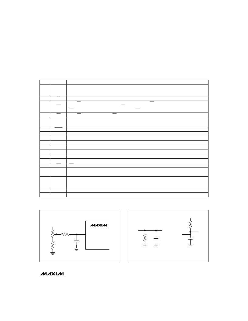
100k
510k
24k
REFADJ
+5V
0.01
μ
F
MAX199
Figure 1. Reference-Adjust Circuit
3k
3k
D
OUT
D
OUT
+5V
a)
High-Z to V
OH
and V
OL
to V
OH
b)
High-Z to V
OL
and V
OH
to V
OL
C
LOAD
C
LOAD
Figure 2. Load Circuits for Enable Time
相关PDF资料 |
PDF描述 |
|---|---|
| MAX2010ETI-T | 500MHz to 1100MHz Adjustable RF Predistorter |
| MAX2014 | 50MHz to 1000MHz, 75dB Logarithmic Detector/Controller |
| MAX2014ETA-T | 50MHz to 1000MHz, 75dB Logarithmic Detector/Controller |
| MAX2015EUA-T | 0.1GHz to 2.5GHz, 75dB Logarithmic Detector/Controller |
| MAX2015 | 0.1GHz to 2.5GHz, 75dB Logarithmic Detector/Controller |
相关代理商/技术参数 |
参数描述 |
|---|---|
| MAX-19H | 制造商:MINI 制造商全称:Mini-Circuits 功能描述:Active Mixer |
| MAX1R | 制造商:Bogen Communications 功能描述:Module, Unbalanced Mono;Input;Screw;RCA;Gain/trim ctrl, mute send and receive 制造商:Bogen Communications 功能描述:AUDIO VISUAL INPUT MODULES; Leaded Process Compatible:No; Peak Reflow Compatible (260 C):No ;RoHS Compliant: No |
| MAX20 | 功能描述:MAX CLIP RoHS:否 类别:风扇,热管理 >> 热敏 - 配件 系列:Max Clip System™ 标准包装:1 系列:- 附件类型:基础组件 适用于相关产品:Intel Pentium II Xeon 其它名称:073974-0004073974-0004-E07397400040739740004-E73974-0004-E739740004739740004-E |
| MAX-20 | 功能描述:保险丝 MAXI FUSE RoHS:否 制造商:Littelfuse 产品:Surface Mount Fuses 电流额定值:0.5 A 电压额定值:600 V 保险丝类型:Fast Acting 保险丝大小/组:Nano 尺寸:12.1 mm L x 4.5 mm W 安装风格: 端接类型:SMD/SMT 系列:485 |
| MAX200 | 制造商:MAXIM 制造商全称:Maxim Integrated Products 功能描述:+5V-Powered, Multichannel RS-232 Drivers/Receivers |
发布紧急采购,3分钟左右您将得到回复。