- 您现在的位置:买卖IC网 > PDF目录9817 > MAX201EWE+T (Maxim Integrated Products)IC TXRX RS-232 W/CAP 16-SOIC PDF资料下载
参数资料
| 型号: | MAX201EWE+T |
| 厂商: | Maxim Integrated Products |
| 文件页数: | 19/23页 |
| 文件大小: | 0K |
| 描述: | IC TXRX RS-232 W/CAP 16-SOIC |
| 产品培训模块: | Lead (SnPb) Finish for COTS Obsolescence Mitigation Program |
| 标准包装: | 1,000 |
| 类型: | 收发器 |
| 驱动器/接收器数: | 2/2 |
| 规程: | RS232 |
| 电源电压: | 4.5 V ~ 5.5 V |
| 安装类型: | 表面贴装 |
| 封装/外壳: | 16-SOIC(0.295",7.50mm 宽) |
| 供应商设备封装: | 16-SOIC W |
| 包装: | 带卷 (TR) |
+5V, RS-232 Transceivers
with 0.1F External Capacitors
Detailed Description
The MAX200–MAX209/MAX211/MAX213 consist of
three sections: charge-pump voltage converters, drivers
(transmitters), and receivers. Each section is described
in detail.
+5V to ±10V Dual Charge-Pump
Voltage Converter
The +5V to Q10V conversion is performed by two
charge-pump voltage converters (Figure 4). The first
uses capacitor C1 to double +5V to +10V, storing +10V
on the V+ output filter capacitor, C3. The second charge-
pump voltage converter uses capacitor C2 to invert +10V
to -10V, storing -10V on the V- output filter capacitor, C4.
The MAX201 and MAX209 include only the V+ to V-
charge pump, and are intended for applications that
have a VCC = +5V supply and a V+ supply in the +9V to
+13.2V range.
In shutdown mode, V+ is internally connected to VCC by
a 1kI pulldown resistor and V- is internally connected to
ground by a 1kI pullup resistor.
RS-232 Drivers
When VCC = +5V, the typical driver output-voltage swing
is Q8V when loaded with a nominal 5kI RS-232 receiver.
The output swing is guaranteed to meet the EIA/TIA-232E
and V.28 specifications, which call for Q5V minimum out-
put levels under worst-case conditions. These include
a minimum 3kI load, VCC = +4.5V, and the maximum
operating temperature. The open-circuit output-voltage
swing ranges from (V+ - 0.6V) to V-.
Input thresholds are both CMOS and TTL compatible.
The inputs of unused drivers can be left unconnected
since 400kI pullup resistors to VCC are included on-
chip. Since all drivers invert, the pullup resistors force
the outputs of unused drivers low. The input pullup resis-
tors typically source 15A; therefore, the driver inputs
should be driven high or open circuited to minimize
power-supply current in shutdown mode.
When in low-power shutdown mode, the driver outputs
are turned off and their leakage current is less than 1mA,
even if the transmitter output is backdriven between 0V
and (VCC + 6V). Below -0.5V, the transmitter output is
diode clamped to ground with a 1kI series impedance.
The transmitter output is also zener clamped to approxi-
mately (VCC + 6V), with a 1kI series impedance.
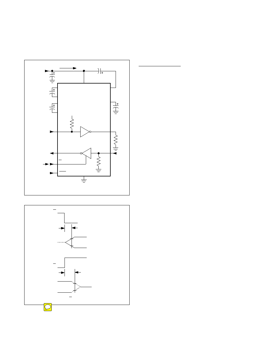
Figure 1. Shutdown Current Test Circuit
Figure 2. Receiver Output Enable and Disable Timing
ISHDN
+5.5V
+5.5V (0)
+5.5V
0V OR +5.5V
DRIVE
0.1FF
C1+
C1-
C2+
C2-
400kI
3kI
5kI
GND
VCC
V+
V-
TIN
+5.5V
T1 T0 T5
R1 T0 R5
TOUT
RIN
0.1FF
SHDN
ROUT
(SHDN)
EN (EN)
MAX200
MAX205
MAX206
MAX211
MAX213
NOTE 1: ( ) ARE FOR MAX213.
NOTE 2: CAPACITORS CAN BE POLARIZED OR UNPOLARIZED.
+3.5V
RECEIVER
OUTPUT
CL = 150pF
+0.8V
VOH - 0.1V
+ 2.5V
VOH
VOL
RL = 1kI
VOL + 0.1V
OUTPUT ENABLE TIME
RECEIVER
OUTPUTS
+3V
0V
EN
INPUT
OUTPUT ENABLE TIME
+3V
0V
EN
INPUT
NOTE: POLARITY OF EN IS REVERSED FOR THE MAX213.
MAX200–MAX209/MAX211/MAX213
Maxim Integrated
5
相关PDF资料 |
PDF描述 |
|---|---|
| VE-2TK-MX-F3 | CONVERTER MOD DC/DC 40V 75W |
| VE-2TK-MX-F2 | CONVERTER MOD DC/DC 40V 75W |
| MAX3483ECSA+T | IC TXRX RS485/422 250KBPS 8-SOIC |
| SY100S314JZ | IC LINE RCVR QUINT DIFF 28-PLCC |
| MAX3490ECSA+T | IC TXRX RS485/422 10MBPS 8SOIC |
相关代理商/技术参数 |
参数描述 |
|---|---|
| MAX202 | 制造商:MAXIM 制造商全称:Maxim Integrated Products 功能描述:+5V-Powered, Multichannel RS-232 Drivers/Receivers |
| MAX202_07 | 制造商:TI 制造商全称:Texas Instruments 功能描述:5-V DUAL RS-232 LINE DRIVER/RECEIVER WITH 【15-kV ESD PROTECTION |
| MAX20-20.0C | 制造商:MDE 制造商全称:MDE Semiconductor, Inc. 功能描述:HIGH CURRENT TRANSIENT VOLTAGE SUPPRESSOR (TVS) DIODE |
| MAX20-20.0CA | 制造商:MDE 制造商全称:MDE Semiconductor, Inc. 功能描述:HIGH CURRENT TRANSIENT VOLTAGE SUPPRESSOR (TVS) DIODE |
| MAX2021 | 制造商:MAXIM 制造商全称:Maxim Integrated Products 功能描述:Evaluation Kit |
发布紧急采购,3分钟左右您将得到回复。