- 您现在的位置:买卖IC网 > PDF目录383344 > MAX2029 (Maxim Integrated Products, Inc.) High-Linearity, 815MHz to 1000MHz Upconversion/ Downconversion Mixer with LO Buffer/Switch PDF资料下载
参数资料
| 型号: | MAX2029 |
| 厂商: | Maxim Integrated Products, Inc. |
| 英文描述: | High-Linearity, 815MHz to 1000MHz Upconversion/ Downconversion Mixer with LO Buffer/Switch |
| 中文描述: | 高线性度、815MHz至1000MHz上变频/下变频混频器,带有LO缓冲/开关 |
| 文件页数: | 13/16页 |
| 文件大小: | 423K |
| 代理商: | MAX2029 |
and LO2 inputs are internally matched to 50
Ω
, requiring
an 82pF DC-blocking capacitor at each input.
A two-stage internal LO buffer allows a wide input-
power range for the LO drive. All guaranteed specifica-
tions are for a -3dBm to +3dBm LO signal power. The
on-chip low-loss balun, along with an LO buffer, drives
the double-balanced mixer. All interfacing and match-
ing components from the LO inputs to the IF outputs
are integrated on-chip.
High-Linearity Mixer
The core of the MAX2029 is a double-balanced, high-
performance passive mixer. Exceptional linearity is pro-
vided by the large LO swing from the on-chip LO buffer.
Differential IF
The MAX2029 mixer has a DC to 250MHz IF frequency
range. Note that these differential ports are ideal for pro-
viding enhanced IIP2 performance. Single-ended IF
applications require a 1:1 balun to transform the 50
Ω
dif-
ferential IF impedance to 50
Ω
single-ended. Including
the balun, the IF return loss is better than 15dB. The dif-
ferential IF is used as an input port for upconverter oper-
ation. The user can use a differential IF amplifier following
the mixer, but a DC block is required on both IF pins.
Applications Information
Input and Output Matching
The RF and LO inputs are internally matched to 50
Ω
. No
matching components are required. As a downconvert-
er, the return loss at the RF port is typically better than
15dB over the entire input range (815MHz to 1000MHz),
and return loss at the LO ports are typically 15dB
(570MHz to 850MHz). RF and LO inputs require only
DC-blocking capacitors for interfacing.
An optional L-C bandpass filter (BPF) can be installed at
the RF port to improve upconverter performance. See
the
Typical Application Circuit
and
Typical Operating
Characteristics
for upconverter operation with an L-C
BPF tuned for 920MHz RF frequency. Performance can
be optimized at other frequencies by choosing different
values for L1 and C4. Removing L1 and C4 altogether
results in a broader match, but performance degrades.
Contact factory for details.
The IF output impedance is 50
Ω
(differential). For eval-
uation, an external low-loss 1:1 (impedance ratio) balun
transforms this impedance to a 50
Ω
single-ended out-
put (see the
Typical Application Circuit).
Bias Resistor
Bias current for the LO buffer is optimized by fine tun-
ing resistor R1. If reduced current is required at the
expense of performance, contact the factory for details.
If the ±1% bias resistor values are not readily available,
substitute standard ±5% values.
Layout Considerations
A properly designed PCB is an essential part of any
RF/microwave circuit. Keep RF signal lines as short as
possible to reduce losses, radiation, and inductance.
For the best performance, route the ground-pin traces
directly to the exposed pad under the package. The
PCB exposed pad
MUST
be connected to the ground
plane of the PCB. It is suggested that multiple vias be
used to connect this pad to the lower-level ground
planes. This method provides a good RF/thermal con-
duction path for the device. Solder the exposed pad on
the bottom of the device package to the PCB. The
MAX2029 evaluation kit can be used as a reference for
board layout. Gerber files are available upon request at
www.maxim-ic.com.
Power-Supply Bypassing
Proper voltage-supply bypassing is essential for high-
frequency circuit stability. Bypass each V
CC
pin with
the capacitors shown in the
Typical Application Circuit
.
See Table 1.
Exposed Pad RF/Thermal Considerations
The exposed paddle (EP) of the MAX2029’s 20-pin thin
QFN-EP package provides a low-thermal-resistance
path to the die. It is important that the PCB on which the
MAX2029 is mounted be designed to conduct heat
from the EP. In addition, provide the EP with a low-
inductance path to electrical ground. The EP
MUST
be
soldered to a ground plane on the PCB, either directly
or through an array of plated via holes.
M
High-Linearity, 815MHz to 1000MHz Upconversion/
Downconversion Mixer with LO Buffer/Switch
______________________________________________________________________________________
13
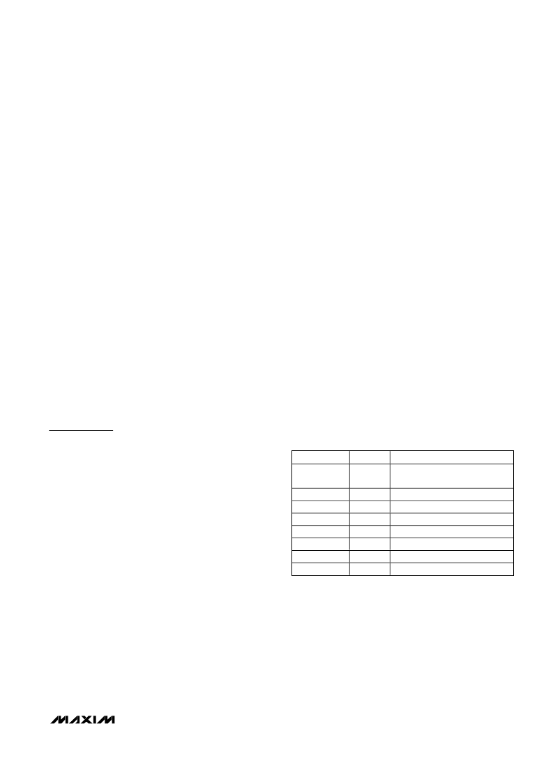
COMPONENT
VALUE
DESCRIPTION
C 1, C 2, C 7, C 8,
C 10, C 11, C12
C3, C6, C9
C4*
C5**
L1*
R1
T1
U1
82pF
Microwave capacitors (0603)
10nF
4.7pF
3.3pF
4.7nH
523
Ω
1:1
MAX2029 Maxim IC
Microwave capacitors (0603)
Microwave capacitor (0603)
Microwave capacitor (0603)
Inductor (0603)
±1% resistor (0603)
IF balun M/A-COM: MABAES0029
Table 1. Typical Application Circuit
Component List
*
C4 and L1 installed only when mixer is used as an upconverter.
**
C5 installed only when mixer is used as a downconverter.
相关PDF资料 |
PDF描述 |
|---|---|
| MAX2031_1 | Evaluation Kit |
| MAX2031EVKIT | Evaluation Kit |
| MAX2031 | High-Linearity, 815MHz to 1000MHz Upconversion/ Downconversion Mixer with LO Buffer/Switch |
| MAX2031ETP | High-Linearity, 815MHz to 1000MHz Upconversion/ Downconversion Mixer with LO Buffer/Switch |
| MAX2034 | Quad-Channel, Ultra-Low-Noise Amplifier with Digitally Programmable Input Impedance |
相关代理商/技术参数 |
参数描述 |
|---|---|
| MAX2029ETP | 功能描述:射频混合器 .815GHz-1GHz Up/Down Mixer RoHS:否 制造商:NXP Semiconductors 频率范围: 转换损失——最大: 工作电源电压:6 V 最大工作温度:+ 85 C 最小工作温度:- 40 C 安装风格:Through Hole 封装 / 箱体:PDIP-8 封装:Tube |
| MAX2029ETP/-T | 制造商:MAXIM 制造商全称:Maxim Integrated Products 功能描述:High-Linearity, 815MHz to 1000MHz Upconversion/ Downconversion Mixer with LO Buffer/Switch |
| MAX2029ETP+ | 功能描述:射频混合器 .815GHz-1GHz Up/Down Mixer RoHS:否 制造商:NXP Semiconductors 频率范围: 转换损失——最大: 工作电源电压:6 V 最大工作温度:+ 85 C 最小工作温度:- 40 C 安装风格:Through Hole 封装 / 箱体:PDIP-8 封装:Tube |
| MAX2029ETP+/+T | 制造商:MAXIM 制造商全称:Maxim Integrated Products 功能描述:High-Linearity, 815MHz to 1000MHz Upconversion/ Downconversion Mixer with LO Buffer/Switch |
| MAX2029ETP+T | 功能描述:射频混合器 .815GHz-1GHz Up/Down Mixer RoHS:否 制造商:NXP Semiconductors 频率范围: 转换损失——最大: 工作电源电压:6 V 最大工作温度:+ 85 C 最小工作温度:- 40 C 安装风格:Through Hole 封装 / 箱体:PDIP-8 封装:Tube |
发布紧急采购,3分钟左右您将得到回复。