- 您现在的位置:买卖IC网 > PDF目录18825 > MAX2055EUP+D (Maxim Integrated)IC ADC DRVR/AMP VAR GAIN 20TSSOP PDF资料下载
参数资料
| 型号: | MAX2055EUP+D |
| 厂商: | Maxim Integrated |
| 文件页数: | 9/13页 |
| 文件大小: | 0K |
| 描述: | IC ADC DRVR/AMP VAR GAIN 20TSSOP |
| 产品培训模块: | Lead (SnPb) Finish for COTS Obsolescence Mitigation Program |
| 标准包装: | 74 |
| 功能: | ADC 驱动器/放大器 |
| 频率: | 30MHz ~ 300MHz |
| RF 型: | 手机,ATE,PHS/PAS |
| 次要属性: | 40dBm 输出 IP3 |
| 封装/外壳: | 20-TSSOP(0.173",4.40mm 宽)裸露焊盘 |
| 包装: | 管件 |
�� �
�
�Digitally� Controlled,� Variable-Gain,� Differential�
�ADC� Driver/Amplifier�
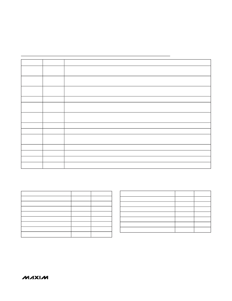
�Pin� Description�
�PIN�
�1,� 9�
�2�
�3,� 18,� 20,� EP�
�4–8�
�10�
�11�
�12�
�13�
�14�
�15�
�16�
�17�
�19�
�NAME�
�V� CC�
�RF_IN�
�GND�
�B4–B0�
�RF_OUT-�
�RF_OUT+�
�I� BIAS�
�C� BP�
�L� E�
�AMP� IN�
�C� C�
�I� SET�
�ATTN� OUT�
�FUNCTION�
�Power� Supply.� Bypass� to� GND� with� capacitors� as� close� to� the� pin� as� possible� as� shown� in� the� typical�
�application� circuits� (Figures� 1� and� 2).�
�Signal� Input.� Internally� matched� to� 50� Ω� over� the� operating� frequency.� See� the� typical� application�
�circuit� for� recommended� component� values.�
�Ground.� Use� low-inductance� layout� techniques� on� the� PC� board.� Solder� the� exposed� paddle� to� the�
�board� ground� plane.�
�Attenuation� Control� Bits.� Digital� input� for� attenuation� control.� See� Table� 3� for� attenuation� setting.�
�Inverted� Differential� Signal� Output.� Requires� an� external� pullup� choke� inductor� (120mA� typical�
�current)� to� V� CC� along� with� a� DC-blocking� capacitor;� see� Figures� 1� and� 2.�
�Noninverted� Differential� Signal� Output.� Requires� an� external� pullup� choke� inductor� (120mA� typical�
�current)� to� V� CC� along� with� a� DC-blocking� capacitor;� see� Figures� 1� and� 2.�
�Amplifier� Bias� Input.� See� Figures� 1� and� 2� for� detailed� connection.�
�Bypass� Capacitor.� See� Figures� 1� and� 2� for� detailed� connection.�
�Amplifier� DC� Ground.� Requires� choke� inductor� that� can� handle� supply� current.� DC� resistance� of�
�inductor� should� be� less� than� 0.2� Ω� .�
�Amplifier� Input.� Requires� DC-coupling� to� allow� biasing.�
�Compensation� Capacitor.� Requires� connection� to� AMP� IN� (pin� 15)� for� stability.�
�Connect� R1� from� I� SET� to� GND� (see� Table� 1� or� Table� 2� for� values).�
�Attenuator� Output.� Requires� external� DC-blocking� capacitor.�
�Table� 1.� Suggested� Components� of�
�Circuit� of� Figure� 1�
�Table� 2.� Suggested� Components� of�
�Circuit� of� Figure� 2�
�COMPONENT�
�C1,� C3–C6,� C8,� C9,� C10,� C12�
�C2,� C11�
�L1,� L3�
�L2�
�L4,� L5�
�R1�
�R7�
�VALUE�
�1nF�
�100pF�
�330nH�
�100nH�
�680nH�
�1.13k� Ω�
�10� Ω�
�SIZE�
�0603�
�0603�
�0603�
�0603�
�1008�
�0603�
�0603�
�COMPONENT�
�C1,� C3,� C4,� C5,� C7–C10,� C12�
�C2,� C11�
�L1,� L2,� L3�
�L4,� L5�
�R1�
�R7�
�T2�
�VALUE�
�1nF�
�100pF�
�330nH�
�680nH�
�909� Ω�
�10� Ω�
�1:1�
�SIZE�
�0603�
�0603�
�0603�
�1008�
�0603�
�0603�
�—�
�T1,� T2�
�1:1�
�—�
�_______________________________________________________________________________________�
�9�
�相关PDF资料 |
PDF描述 |
|---|---|
| CM421255 | SCR MOD PWR-BLK 1200V 55A |
| MAX9990ETP+ | IC BUFFER LO 20-TQFN |
| T620023004DN | SCR PHASE CTRL MOD 200V 300A |
| MAX2620EUA+ | IC RF OSC W/BUFFERED OUT 8-UMAX |
| MAX2623EUA+ | IC SELF-CONTAINED VCO 8-MSOP |
相关代理商/技术参数 |
参数描述 |
|---|---|
| MAX2055EUP-T | 制造商:Maxim Integrated Products 功能描述:DIGITALLY CONTROLLED, VARIABLE-GAIN, DIFFEREN - Tape and Reel |
| MAX2055EUP-TD | 功能描述:射频放大器 RoHS:否 制造商:Skyworks Solutions, Inc. 类型:Low Noise Amplifier 工作频率:2.3 GHz to 2.8 GHz P1dB:18.5 dBm 输出截获点:37.5 dBm 功率增益类型:32 dB 噪声系数:0.85 dB 工作电源电压:5 V 电源电流:125 mA 测试频率:2.6 GHz 最大工作温度:+ 85 C 安装风格:SMD/SMT 封装 / 箱体:QFN-16 封装:Reel |
| MAX2055EVKIT | 功能描述:射频放大器 RoHS:否 制造商:Skyworks Solutions, Inc. 类型:Low Noise Amplifier 工作频率:2.3 GHz to 2.8 GHz P1dB:18.5 dBm 输出截获点:37.5 dBm 功率增益类型:32 dB 噪声系数:0.85 dB 工作电源电压:5 V 电源电流:125 mA 测试频率:2.6 GHz 最大工作温度:+ 85 C 安装风格:SMD/SMT 封装 / 箱体:QFN-16 封装:Reel |
| MAX2056 | 制造商:MAXIM 制造商全称:Maxim Integrated Products 功能描述:Evaluation Kit |
| MAX2056_1 | 制造商:MAXIM 制造商全称:Maxim Integrated Products 功能描述:Evaluation Kit |
发布紧急采购,3分钟左右您将得到回复。