- 您现在的位置:买卖IC网 > PDF目录18754 > MAX2057ETX+T (Maxim Integrated)IC AMP VARIABLE GAIN 36-TQFN PDF资料下载
参数资料
| 型号: | MAX2057ETX+T |
| 厂商: | Maxim Integrated |
| 文件页数: | 11/13页 |
| 文件大小: | 0K |
| 描述: | IC AMP VARIABLE GAIN 36-TQFN |
| 产品培训模块: | Lead (SnPb) Finish for COTS Obsolescence Mitigation Program |
| 标准包装: | 2,500 |
| 频率: | 1.7GHz ~ 2.5GHz |
| P1dB: | 23.8dBm(239.9mW) |
| 增益: | 13.5dB ~ 17.5dB |
| 噪音数据: | 6dB |
| RF 型: | 手机,ATE,GSM,EDGE,ISM,W-CDMA,802.16/WiMax,CDMA2000 |
| 电源电压: | 4.75 V ~ 5.25 V |
| 电流 - 电源: | 180mA ~ 230mA |
| 测试频率: | 2.1GHz |
| 封装/外壳: | 36-WFQFN 裸露焊盘 |
| 包装: | 带卷 (TR) |
�� �
�
�1300MHz� to� 2700MHz� Variable-Gain�
�Amplifier� with� Analog� Gain� Control�
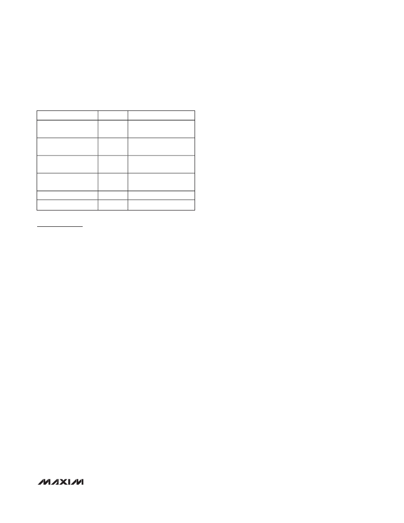
�Table� 1.� Typical� Application� Circuit�
�Component� Values�
�Amplifier� Bias� Current�
�The� MAX2057� integrates� a� two-stage� amplifier� to� simul-�
�taneously� provide� high� gain� and� high� IP3.� Optimal� per-�
�DESIGNATION�
�C1,� C3,� C5,� C7,� C10�
�C2,� C4,� C6,� C8,� C9�
�C13,� C14,� C15�
�C17�
�R1�
�R2�
�VALUE�
�22pF�
�1000pF�
�0.1μF�
�0.75pF�
�1.2k� ?�
�2k� ?�
�TYPE�
�Microwave� capacitors�
�(0402)�
�Microwave� capacitors�
�(0402)�
�Microwave� capacitors�
�(0603)�
�Microwave� capacitor�
�(0402)�
�±1%� resistor� (0402)�
�±1%� resistor� (0402)�
�formance� is� obtained� when� R1� and� R2� are� equal� to�
�1.2k� ?� and� 2k� ?� ,� respectively.� The� typical� supply� current�
�is� 180mA� and� the� typical� output� IP3� is� 37dBm� under�
�these� conditions.�
�Increasing� R� 1� and� R� 2� from� the� nominal� values� of� 1.2k� ?�
�and� 2k� ?� reduces� the� bias� current� of� each� amplifier�
�stage,� which� reduces� the� total� power� consumption� and�
�IP3� of� the� device.� This� feature� can� be� utilized� to� further�
�decrease� power� consumption� for� applications� that� do�
�not� require� high� IP3.�
�Layout� Considerations�
�A� properly� designed� PC� board� is� an� essential� part� of�
�any� RF/microwave� circuit.� Keep� RF� signal� lines� as� short�
�as� possible� to� reduce� losses,� radiation,� and� induc-�
�Applications� Information�
�Analog� Attenuation� Control�
�A� single� input� voltage� at� the� V� CNTL� pin� adjusts� the� gain�
�of� the� MAX2057.� Up� to� 21dB� of� gain-control� range� is�
�provided� through� a� single� attenuator.� At� the� maximum�
�gain� setting,� each� attenuator’s� insertion� loss� is� approxi-�
�mately� 2.2dB.� With� the� single� attenuator� at� the� maximum�
�gain� setting,� the� device� provides� a� nominal� 15.5dB� of�
�cascaded� gain� and� 6dB� of� cascaded� noise� figure.�
�If� a� larger� gain-control� range� is� desired,� a� second� on-�
�chip� attenuator� can� be� connected� in� the� signal� path� to�
�provide� an� additional� 21dB� of� gain-control� range.� With�
�the� second� attenuator� connected� at� the� maximum� gain�
�setting,� the� device� typically� exhibits� 13.3dB� of� cascad-�
�ed� gain.� Note� that� the� V� CNTL� pin� simultaneously� adjusts�
�both� on-chip� attenuators.�
�The� V� CNTL� input� voltage� drives� a� high-impedance� load�
�(>� 50k� ?� ).� It� is� suggested� that� a� current-limiting� resistor�
�be� included� in� series� with� this� connection� to� limit� the�
�input� current� to� less� than� 40mA� should� the� control� volt-�
�age� be� applied� when� V� CC� is� not� present.� A� series� resis-�
�tor� of� greater� than� 200� ?� will� provide� complete�
�protection� for� 5V� control� voltage� ranges.� Limit� V� CNTL�
�input� voltages� to� a� 1.0V� to� 4.5V� range� when� V� CC� is�
�present� to� ensure� the� reliability� of� the� device.�
�tance.� For� best� performance,� route� the� ground-pin�
�traces� directly� to� the� exposed� pad� underneath� the�
�package.� This� pad� MUST� be� connected� to� the� ground�
�plane� of� the� board� by� using� multiple� vias� under� the�
�device� to� provide� the� best� RF� and� thermal� conduction�
�path.� Solder� the� exposed� pad� on� the� bottom� of� the�
�device� package� to� a� PC� board� exposed� pad.�
�Power-Supply� Bypassing�
�Proper� voltage-supply� bypassing� is� essential� for� high-�
�frequency� circuit� stability.� Bypass� each� V� CC� pin� with�
�capacitors� placed� as� close� to� the� device� as� possible.�
�Place� the� smallest� capacitor� closest� to� the� device.� Refer�
�to� the� MAX2057� evaluation� kit� data� sheet� for� more� details.�
�Exposed� Pad� RF� and� Thermal�
�Considerations�
�The� EP� of� the� MAX2057’s� 36-pin� thin� QFN-EP� package�
�provides� a� low-thermal-resistance� path� to� the� die.� It� is�
�important� that� the� PC� board� on� which� the� IC� is� mounted�
�be� designed� to� conduct� heat� from� this� contact.� In� addi-�
�tion,� the� EP� provides� a� low-inductance� RF� ground� path�
�for� the� device.�
�The� EP� MUST� be� soldered� to� a� ground� plane� on� the� PC�
�board� either� directly� or� through� an� array� of� plated� via�
�holes.� Soldering� the� pad� to� ground� is� also� critical� for�
�efficient� heat� transfer.� Use� a� solid� ground� plane� wher-�
�ever� possible.�
�______________________________________________________________________________________�
�11�
�相关PDF资料 |
PDF描述 |
|---|---|
| IF-6-20 | XFRMR 115/230V 10V 600MA 6VA PCB |
| MAX2056ETX+T | IC AMP VARIABLE GAIN 36-TQFN |
| MAX2066ETL+T | IC VGA PROG DIGITAL 40TQFN-EP |
| MAX2265EUE+ | IC AMP POWER CELL 16TSSOP-EP |
| IF-6-16 | XFRMR 115/230V 8V 750MA 6VA PCB |
相关代理商/技术参数 |
参数描述 |
|---|---|
| MAX2057EVKIT | 功能描述:放大器 IC 开发工具 RoHS:否 制造商:International Rectifier 产品:Demonstration Boards 类型:Power Amplifiers 工具用于评估:IR4302 工作电源电压:13 V to 23 V |
| MAX2058 | 制造商:MAXIM 制造商全称:Maxim Integrated Products 功能描述:700MHz to 1200MHz High-Linearity, SPI-Controlled DVGA with Integrated Loopback Mixer |
| MAX2058ETL | 功能描述:射频放大器 0.7GHz - 1.2GHz SPI-Controlled DVGA RoHS:否 制造商:Skyworks Solutions, Inc. 类型:Low Noise Amplifier 工作频率:2.3 GHz to 2.8 GHz P1dB:18.5 dBm 输出截获点:37.5 dBm 功率增益类型:32 dB 噪声系数:0.85 dB 工作电源电压:5 V 电源电流:125 mA 测试频率:2.6 GHz 最大工作温度:+ 85 C 安装风格:SMD/SMT 封装 / 箱体:QFN-16 封装:Reel |
| MAX2058ETL+ | 功能描述:射频放大器 0.7GHz - 1.2GHz SPI-Controlled DVGA RoHS:否 制造商:Skyworks Solutions, Inc. 类型:Low Noise Amplifier 工作频率:2.3 GHz to 2.8 GHz P1dB:18.5 dBm 输出截获点:37.5 dBm 功率增益类型:32 dB 噪声系数:0.85 dB 工作电源电压:5 V 电源电流:125 mA 测试频率:2.6 GHz 最大工作温度:+ 85 C 安装风格:SMD/SMT 封装 / 箱体:QFN-16 封装:Reel |
| MAX2058ETL+T | 功能描述:射频放大器 0.7GHz - 1.2GHz SPI-Controlled DVGA RoHS:否 制造商:Skyworks Solutions, Inc. 类型:Low Noise Amplifier 工作频率:2.3 GHz to 2.8 GHz P1dB:18.5 dBm 输出截获点:37.5 dBm 功率增益类型:32 dB 噪声系数:0.85 dB 工作电源电压:5 V 电源电流:125 mA 测试频率:2.6 GHz 最大工作温度:+ 85 C 安装风格:SMD/SMT 封装 / 箱体:QFN-16 封装:Reel |
发布紧急采购,3分钟左右您将得到回复。