- 您现在的位置:买卖IC网 > PDF目录18754 > MAX2064ETM+T (Maxim Integrated)IC VGA PROG ANALOG 48TQFN-EP PDF资料下载
参数资料
| 型号: | MAX2064ETM+T |
| 厂商: | Maxim Integrated |
| 文件页数: | 2/20页 |
| 文件大小: | 0K |
| 描述: | IC VGA PROG ANALOG 48TQFN-EP |
| 产品培训模块: | Lead (SnPb) Finish for COTS Obsolescence Mitigation Program |
| 标准包装: | 2,500 |
| 频率: | 50MHz ~ 1GHz |
| P1dB: | 18.7dBm |
| 增益: | 20.6dB |
| 噪音数据: | 5.7dB |
| RF 型: | 通用 |
| 电源电压: | 3.135 V ~ 3.465 V,4.75 V ~ 5.25 V |
| 电流 - 电源: | 143mA |
| 测试频率: | 900MHz |
| 封装/外壳: | 48-WFQFN 裸露焊盘 |
| 包装: | 带卷 (TR) |
�� �
�
�Dual� 50MHz� to� 1000MHz� High-Linearity,�
�Serial/Analog-Controlled� VGA�
�ABSOLUTE� MAXIMUM� RATINGS�
�V� CC_AMP_1� ,� V� CC_AMP_2� ,� V� CC_RG� to� GND� ..........-0.3V� to� +5.5V�
�PD_1,� PD_2,� AMPSET� to� GND� .............................-0.3V� to� +3.6V�
�A_VCTL_1,� A_VCTL_2� to� GND� .............................-0.3V� to� +3.6V�
�DAT,� CS� ,� CLK,� AA_SP� to� GND� ............................-0.3V� to� +3.6V�
�AMP_IN_1,� AMP_IN_2� to� GND� ..........................+0.95V� to� +1.2V�
�AMP_OUT_1,� AMP_OUT_2� to� GND� .....................-0.3V� to� +5.5V�
�A_ATT_IN_1,� A_ATT_IN_2,� A_ATT_OUT_1,�
�A_ATT_OUT_2� to� GND� .........................................� 0V� to� +3.6V�
�REG_OUT� to� GND� ................................................-0.3V� to� +3.6V�
�RF� Input� Power� (A_ATT_IN_1,� A_ATT_IN_2).................� +20dBm�
�RF� Input� Power� (AMP_IN_1,� AMP_IN_2).......................� +18dBm�
�q� JC� (Notes� 1,� 2)� .........................................................� +12.3� N� C/W�
�q� JA� (Notes� 2,� 3)� ............................................................� +38� N� C/W�
�Continuous� Power� Dissipation� (Note� 1)� ..............................5.3W�
�Operating� Case� Temperature� Range� (Note� 4)� ..� -40� N� C� to� +85� N� C�
�Junction� Temperature� .....................................................+150� N� C�
�Storage� Temperature� Range............................� -65� N� C� to� +150� N� C�
�Lead� Temperature� (soldering,� 10s)� ................................+300� N� C�
�Soldering� Temperature� (reflow)� ......................................+260� N� C�
�Note� 1:� Based� on� junction� temperature� T� J� =� T� C� +� (� q� JC� x� V� CC� x� I� CC� ).� This� formula� can� be� used� when� the� temperature� of� the�
�exposed� pad� is� known� while� the� device� is� soldered� down� to� a� PCB.� See� the� Applications� Information� section� for� details.�
�The� junction� temperature� must� not� exceed� +150� N� C.�
�Note� 2:� Package� thermal� resistances� were� obtained� using� the� method� described� in� JEDEC� specification� JESD51-7,� using� a� four-�
�layer� board.� For� detailed� information� on� package� thermal� considerations,� refer� to� www.maxim-ic.com/thermal-tutorial� .�
�Note� 3:� Junction� temperature� T� J� =� T� A� +� (� q� JA� x� V� CC� x� I� CC� ).� This� formula� can� be� used� when� the� ambient� temperature� of� the� PCB� is�
�known.� The� junction� temperature� must� not� exceed� +150� N� C.�
�Note� 4:� T� C� is� the� temperature� on� the� exposed� pad� of� the� package.� T� A� is� the� ambient� temperature� of� the� device� and� PCB.�
�Stresses� beyond� those� listed� under� “Absolute� Maximum� Ratings”� may� cause� permanent� damage� to� the� device.� These� are� stress� ratings� only,� and� functional�
�operation� of� the� device� at� these� or� any� other� conditions� beyond� those� indicated� in� the� operational� sections� of� the� specifications� is� not� implied.� Exposure� to� absolute�
�maximum� rating� conditions� for� extended� periods� may� affect� device� reliability.�
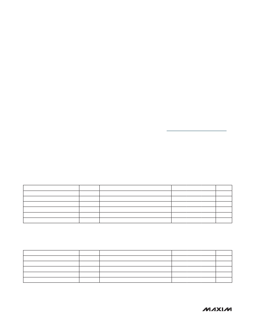
�+5V� SUPPLY� DC� ELECTRICAL� CHARACTERISTICS�
�(� Typical� Application� Circuit� ,� V� CC� =� V� CC_AMP_1� =� V� CC_AMP_2� =� V� CC_RG� =� +4.75V� to� +5.25V,� AMPSET� =� 0,� PD_1� =� PD_2� =� 0,�
�T� C� =� -40� N� C� to� +85� N� C.� Typical� values� are� at� V� CC_� =� +5.0V� and� T� C� =� +25� N� C,� unless� otherwise� noted.)�
�PARAMETER�
�Supply� Voltage�
�Supply� Current�
�Power-Down� Current�
�SYMBOL�
�V� CC�
�I� DC�
�I� DCPD�
�CONDITIONS�
�PD_1� =� PD_2� =� 1,� V� IH� =� 3.3V�
�MIN�
�4.75�
�TYP�
�5�
�143�
�5.3�
�MAX�
�5.25�
�210�
�8�
�UNITS�
�V�
�mA�
�mA�
�Input� Low� Voltage�
�V� IL�
�0.5�
�V�
�Input� High� Voltage�
�Input� Logic� Current�
�V� IH�
�I� IH,� I� IL�
�1.7�
�-1�
�3.465�
�+1�
�V�
�F� A�
�+3.3V� SUPPLY� DC� ELECTRICAL� CHARACTERISTICS�
�(� Typical� Application� Circuit� ,� V� CC� =� V� CC_AMP_1� =� V� CC_AMP_2� =� V� CC_RG� =� +3.135V� to� +3.465V,� AMPSET� =� 1,� PD_1� =� PD_2� =� 0,�
�T� C� =� -40� N� C� to� +85� N� C.� Typical� values� are� at� V� CC_� =� +3.3V� and� T� C� =� +25� N� C,� unless� otherwise� noted.)�
�PARAMETER�
�Supply� Voltage�
�Supply� Current�
�Power-Down� Current�
�SYMBOL�
�V� CC�
�I� DC�
�I� DCPD�
�CONDITIONS�
�PD_1� =� PD_2� =� 1,� V� IH� =� 3.3V�
�MIN�
�3.135�
�TYP�
�3.3�
�84.7�
�4.5�
�MAX�
�3.465�
�145�
�8�
�UNITS�
�V�
�mA�
�mA�
�Input� Low� Voltage�
�Input� High� Voltage�
�V� IL�
�V� IH�
�0.5�
�1.7�
�V�
�V�
�2�
�______________________________________________________________________________________�
�相关PDF资料 |
PDF描述 |
|---|---|
| MAX2063ETM+T | IC VGA PROG DIGITAL 48TQFN-EP |
| IF-6-40 | XFRMR 115/230V 20V 300MA 6VA PCB |
| GLDB01A1Y | SWITCH ROTARY SIDE |
| MAX2059ETL+T | IC DVGA SPI HI LIN 40-TQFN |
| IF-6-34 | XFRMR 115/230V 17V 360MA 6VA PCB |
相关代理商/技术参数 |
参数描述 |
|---|---|
| MAX2064EVKIT# | 功能描述:放大器 IC 开发工具 MAX2064 Eval Kit RoHS:否 制造商:International Rectifier 产品:Demonstration Boards 类型:Power Amplifiers 工具用于评估:IR4302 工作电源电压:13 V to 23 V |
| MAX2065 | 制造商:MAXIM 制造商全称:Maxim Integrated Products 功能描述:50MHz to 1000MHz High-Linearity, Serial/ Parallel-Controlled Analog/Digital VGA |
| MAX2065ETL+ | 功能描述:射频放大器 Dl 50-1000MHz Hi-Lin Analog/Digital VGA RoHS:否 制造商:Skyworks Solutions, Inc. 类型:Low Noise Amplifier 工作频率:2.3 GHz to 2.8 GHz P1dB:18.5 dBm 输出截获点:37.5 dBm 功率增益类型:32 dB 噪声系数:0.85 dB 工作电源电压:5 V 电源电流:125 mA 测试频率:2.6 GHz 最大工作温度:+ 85 C 安装风格:SMD/SMT 封装 / 箱体:QFN-16 封装:Reel |
| MAX2065ETL+T | 功能描述:射频放大器 Dl 50-1000MHz Hi-Lin Analog/Digital VGA RoHS:否 制造商:Skyworks Solutions, Inc. 类型:Low Noise Amplifier 工作频率:2.3 GHz to 2.8 GHz P1dB:18.5 dBm 输出截获点:37.5 dBm 功率增益类型:32 dB 噪声系数:0.85 dB 工作电源电压:5 V 电源电流:125 mA 测试频率:2.6 GHz 最大工作温度:+ 85 C 安装风格:SMD/SMT 封装 / 箱体:QFN-16 封装:Reel |
| MAX2065EVKIT | 功能描述:射频放大器 RF and RFID RF Evaluation & Development Kits & Boards - KIT EVALUATION FOR MAX2065 RoHS:否 制造商:Skyworks Solutions, Inc. 类型:Low Noise Amplifier 工作频率:2.3 GHz to 2.8 GHz P1dB:18.5 dBm 输出截获点:37.5 dBm 功率增益类型:32 dB 噪声系数:0.85 dB 工作电源电压:5 V 电源电流:125 mA 测试频率:2.6 GHz 最大工作温度:+ 85 C 安装风格:SMD/SMT 封装 / 箱体:QFN-16 封装:Reel |
发布紧急采购,3分钟左右您将得到回复。