- 您现在的位置:买卖IC网 > Datasheet目录472 > MAX2066EVKIT (Maxim Integrated)KIT EVALUATION FOR MAX2066 Datasheet资料下载
参数资料
| 型号: | MAX2066EVKIT |
| 厂商: | Maxim Integrated |
| 文件页数: | 2/23页 |
| 文件大小: | 0K |
| 描述: | KIT EVALUATION FOR MAX2066 |
| 产品培训模块: | Lead (SnPb) Finish for COTS Obsolescence Mitigation Program |
| 标准包装: | 1 |
| 类型: | 放大器 |
| 频率: | 50MHz ~ 1GHz |
| 适用于相关产品: | MAX2066 |
| 已供物品: | 板 |
�� �
�
�50MHz� to� 1000MHz� High-Linearity,�
�Serial/Parallel-Controlled� Digital� VGA�
�ABSOLUTE� MAXIMUM� RATINGS�
�VCC_� to� GND� ........................................................-0.3V� to� +5.5V�
�VDD_LOGIC,� DATA,� CS� ,� CLK,�
�SER/PAR..............................................-0.3V� to� (VCC_� +� 0.3V)�
�STATE_A,� STATE_B,� D0–D4� ....................-0.3V� to� (VCC_� +� 0.3V)�
�AMP_IN,� AMP_OUT� .................................-0.3V� to� (VCC_� +� 0.3V)�
�ATTEN_IN,� ATTEN_OUT........................................-1.2V� to� +1.2V�
�RSET� to� GND.........................................................-0.3V� to� +1.2V�
�RF� Input� Power� (ATTEN_IN,� ATTEN_OUT).....................+20dBm�
�RF� Input� Power� (AMP_IN)...............................................+18dBm�
�Continuous� Power� Dissipation� (Note� 1)� ...............................6.5W�
�θ� JA� (Notes� 2,� 3)..............................................................+38°C/W�
�θ� JC� (Note� 3)� ...................................................................+10°C/W�
�Operating� Temperature� Range� (Note� 4)� .....T� C� =� -40°C� to� +85°C�
�Maximum� Junction� Temperature� .....................................+150°C�
�Storage� Temperature� Range� .............................-65°C� to� +150°C�
�Lead� Temperature� (soldering,� 10s)� .................................+300°C�
�Note� 1:� Based� on� junction� temperature� T� J� =� T� C� +� (� θ� JC� x� V� CC� x� I� CC� ).� This� formula� can� be� used� when� the� temperature� of� the� exposed�
�pad� is� known� while� the� device� is� soldered� down� to� a� printed-circuit� board� (PCB).� See� the� Applications� Information� section�
�for� details.� The� junction� temperature� must� not� exceed� +150°C.�
�Note� 2:� Junction� temperature� T� J� =� T� A� +� (� θ� JA� x� V� CC� x� I� CC� ).� This� formula� can� be� used� when� the� ambient� temperature� of� the� PCB� is�
�known.� The� junction� temperature� must� not� exceed� +150°C.�
�Note� 3:� Package� thermal� resistances� were� obtained� using� the� method� described� in� JEDEC� specification� JESD51-7,� using� a� 4-layer�
�board.� For� detailed� information� on� package� thermal� considerations,� refer� to� www.maxim-ic.com/thermal-tutorial� .�
�Note� 4:� T� C� is� the� temperature� on� the� exposed� pad� of� the� package.� T� A� is� the� ambient� temperature� of� the� device� and� PCB.�
�Stresses� beyond� those� listed� under� “Absolute� Maximum� Ratings”� may� cause� permanent� damage� to� the� device.� These� are� stress� ratings� only,� and� functional�
�operation� of� the� device� at� these� or� any� other� conditions� beyond� those� indicated� in� the� operational� sections� of� the� specifications� is� not� implied.� Exposure� to�
�absolute� maximum� rating� conditions� for� extended� periods� may� affect� device� reliability.�
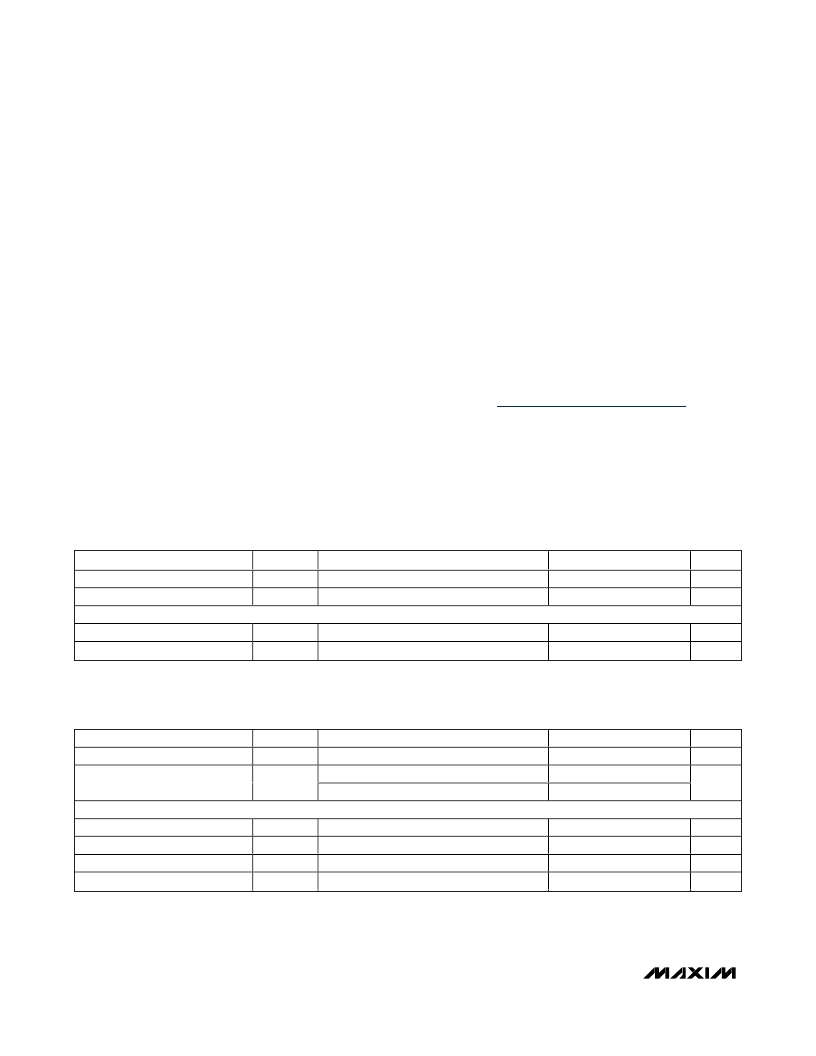
�+3.3V� SUPPLY� DC� ELECTRICAL� CHARACTERISTICS�
�(Typical� Application� Circuit,� high-current� (HC)� mode,� V� CC� =� V� DD� =� +3.0V� to� +3.6V,� T� C� =� -40°C� to� +85°C.� Typical� values� are� at� V� CC� =�
�V� DD� =� +3.3V� and� T� C� =� +25°C,� unless� otherwise� noted.)�
�PARAMETER�
�Supply� Voltage�
�Supply� Current�
�SYMBOL�
�V� CC�
�I� CC�
�(Note� 5)�
�CONDITIONS�
�MIN�
�3.0�
�TYP�
�3.3�
�58�
�MAX�
�3.6�
�80�
�UNITS�
�V�
�mA�
�LOGIC INPUTS (DATA,� CS� , CLK,� SER/PAR,� STATE_A,� STATE_B,� D0� –� D4)�
�Input� High� Voltage�
�Input� Low� Voltage�
�V� IH�
�V� IL�
�2�
�0.8�
�V�
�V�
�+5V� SUPPLY� DC� ELECTRICAL� CHARACTERISTICS�
�(Typical� Application� Circuit,� V� CC� =� V� DD� =� +4.75V� to� +5.25V,� T� C� =� -40°C� to� +85°C.� Typical� values� are� at� V� CC� =� V� DD� =� +5V� and�
�T� C� =� +25°C,� unless� otherwise� noted.)�
�PARAMETER�
�SYMBOL�
�CONDITIONS�
�MIN�
�TYP�
�MAX�
�UNITS�
�Supply� Voltage�
�Supply� Current�
�V� CC�
�I� CC�
�Low-current� (LC)� mode�
�High-current� (HC)� mode�
�4.75�
�5�
�70�
�121�
�5.25�
�90�
�144�
�V�
�mA�
�LOGIC INPUTS (DATA,� CS� , CLK,� SER/PAR,� STATE_A,� STATE_B,� D0� –� D4)�
�Input� High� Voltage�
�Input� Low� Voltage�
�V� IH�
�V� IL�
�3�
�0.8�
�V�
�V�
�Input� Current� Logic-High�
�Input� Current� Logic-Low�
�I� IH�
�I� IL�
�-1�
�-1�
�+1�
�+1�
�μA�
�μA�
�2�
�_______________________________________________________________________________________�
�相关PDF资料 |
PDF描述 |
|---|---|
| MAX2067EVKIT | KIT EVALUATION FOR MAX2067 |
| MAX2091ETP+T | IC UPCONVERTING MIXER 20TQFN |
| MAX2092ETP+T | IC UPCONVERTING MIXER 20TQFN |
| MAX2112EVKIT+ | KIT EVAL FOR MAX2112 |
| MAX2116EVKIT+ | KIT EVAL FOR MAX2116 |
相关代理商/技术参数 |
参数描述 |
|---|---|
| MAX2066EVKIT# | 功能描述:射频放大器 RoHS:否 制造商:Skyworks Solutions, Inc. 类型:Low Noise Amplifier 工作频率:2.3 GHz to 2.8 GHz P1dB:18.5 dBm 输出截获点:37.5 dBm 功率增益类型:32 dB 噪声系数:0.85 dB 工作电源电压:5 V 电源电流:125 mA 测试频率:2.6 GHz 最大工作温度:+ 85 C 安装风格:SMD/SMT 封装 / 箱体:QFN-16 封装:Reel |
| MAX2067ETL+ | 功能描述:射频放大器 Dl 50-1000MHz Hi-Lin Analog/Digital VGA RoHS:否 制造商:Skyworks Solutions, Inc. 类型:Low Noise Amplifier 工作频率:2.3 GHz to 2.8 GHz P1dB:18.5 dBm 输出截获点:37.5 dBm 功率增益类型:32 dB 噪声系数:0.85 dB 工作电源电压:5 V 电源电流:125 mA 测试频率:2.6 GHz 最大工作温度:+ 85 C 安装风格:SMD/SMT 封装 / 箱体:QFN-16 封装:Reel |
| MAX2067ETL+T | 功能描述:射频放大器 Dl 50-1000MHz Hi-Lin Analog/Digital VGA RoHS:否 制造商:Skyworks Solutions, Inc. 类型:Low Noise Amplifier 工作频率:2.3 GHz to 2.8 GHz P1dB:18.5 dBm 输出截获点:37.5 dBm 功率增益类型:32 dB 噪声系数:0.85 dB 工作电源电压:5 V 电源电流:125 mA 测试频率:2.6 GHz 最大工作温度:+ 85 C 安装风格:SMD/SMT 封装 / 箱体:QFN-16 封装:Reel |
| MAX2067EVKIT | 功能描述:射频放大器 RF and RFID RF Evaluation & Development Kits & Boards - KIT EVALUATION FOR MAX2067 RoHS:否 制造商:Skyworks Solutions, Inc. 类型:Low Noise Amplifier 工作频率:2.3 GHz to 2.8 GHz P1dB:18.5 dBm 输出截获点:37.5 dBm 功率增益类型:32 dB 噪声系数:0.85 dB 工作电源电压:5 V 电源电流:125 mA 测试频率:2.6 GHz 最大工作温度:+ 85 C 安装风格:SMD/SMT 封装 / 箱体:QFN-16 封装:Reel |
| MAX2067EVKIT# | 功能描述:射频放大器 RoHS:否 制造商:Skyworks Solutions, Inc. 类型:Low Noise Amplifier 工作频率:2.3 GHz to 2.8 GHz P1dB:18.5 dBm 输出截获点:37.5 dBm 功率增益类型:32 dB 噪声系数:0.85 dB 工作电源电压:5 V 电源电流:125 mA 测试频率:2.6 GHz 最大工作温度:+ 85 C 安装风格:SMD/SMT 封装 / 箱体:QFN-16 封装:Reel |
发布紧急采购,3分钟左右您将得到回复。