- 您现在的位置:买卖IC网 > Datasheet目录472 > MAX2411AEEI+ (Maxim Integrated)IC UP/DOWNCONVERTER 28-QSOP Datasheet资料下载
参数资料
| 型号: | MAX2411AEEI+ |
| 厂商: | Maxim Integrated |
| 文件页数: | 9/14页 |
| 文件大小: | 0K |
| 描述: | IC UP/DOWNCONVERTER 28-QSOP |
| 产品培训模块: | Lead (SnPb) Finish for COTS Obsolescence Mitigation Program |
| 标准包装: | 50 |
| 功能: | 升/降频器,LNA,PA 驱动器 |
| 频率: | 1.9GHz |
| RF 型: | DCS1800/PCS1900,DECT,ISM,PHS/PACS,PWT1900 |
| 次要属性: | 3.2dB 组合接收器噪声系数 |
| 封装/外壳: | 28-QSOP |
| 包装: | 管件 |
�� �
�
�Low-Cost� RF� Up/Downconverter�
�with� LNA� and� PA� Driver�
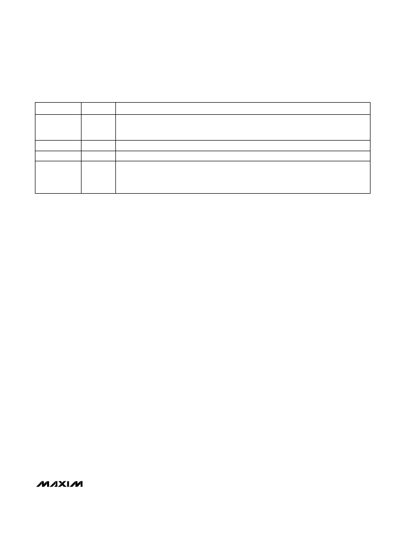
�_________________________________________________Pin� Description� (continued)�
�PIN�
�24�
�25�
�26�
�27�
�NAME�
�RXMXIN�
�GND�
�GND�
�LNAOUT�
�FUNCTION�
�RF� Input� to� Receive� Mixer� (downconverter).� This� input� typically� requires� a� matching� network� for�
�connecting� to� an� external� filter.� AC� couple� to� this� pin.� See� the� Typical� Operating� Characteristics�
�for� a� plot� of� RXMXIN� Impedance� vs.� Frequency.�
�Receive� Mixer� Input� Ground.� Connect� GND� to� the� PC� board� ground� plane� with� minimal� inductance.�
�LNA� Output� Ground.� Connect� GND� to� the� PC� board� ground� plane� with� minimal� inductance.�
�LNA� Output.� AC� couple� to� this� pin.� This� output� typically� provides� a� VSWR� of� better� than� 2:1� at� fre-�
�quencies� from� 1.7GHz� to� 3GHz� with� no� external� matching� components.� At� other� frequencies,� a�
�matching� network� may� be� required� to� match� LNAOUT� to� an� external� filter.� Consult� the� Typical�
�Operating� Characteristics� for� a� plot� of� LNA� Output� Impedance� vs.� Frequency.�
�_______________Detailed� Description�
�The� MAX2411A� consists� of� five� major� components:� a�
�transmit� mixer� followed� by� a� variable-gain� power-�
�amplifier� (PA)� driver� as� well� as� a� low-noise� amplifier�
�(LNA),� receive� mixer,� and� power-management� section.�
�The� following� sections� describe� each� of� the� blocks� in�
�the� MAX2411A� Functional� Diagram.�
�Low-Noise� Amplifier� (LNA)�
�The� LNA� is� a� wideband,� single-ended� cascode� amplifi-�
�er� that� can� be� used� over� a� wide� range� of� frequencies.�
�Refer� to� the� LNA� Gain� vs.� Frequency� graph� in� the�
�Typical� Operating� Characteristics.� Its� port� impedances�
�are� optimized� for� operation� around� 1.9GHz,� requiring�
�only� a� 1pF� shunt� capacitor� at� the� LNA� input� for� a� VSWR�
�of� better� than� 2:1� and� a� noise� figure� of� 2.4dB.� As� with�
�every� LNA,� the� input� match� can� be� traded� off� for� better�
�noise� figure.�
�PA� Driver�
�The� PA� driver� has� typically� 15dB� of� gain,� which� is�
�adjustable� over� a� 35dB� range� via� the� GC� pin.� At� full� gain,�
�the� PA� driver� has� a� noise� figure� of� 3.5dB� at� 1.9GHz.�
�For� input� and� output� matching� information,� refer� to� the�
�Typical� Operating� Characteristics� for� plots� of� PA� Driver�
�Input� and� Output� Impedance� vs.� Frequency.�
�Bidirectional� IF� Port�
�The� MAX2411A� has� a� unique� bidirectional� differential� IF�
�port,� which� can� eliminate� the� need� for� separate� transmit�
�and� receive� IF� filters,� reducing� cost� and� component� count.�
�Consult� the� Typical� Operating� Circuit� for� more� information.�
�For� single-ended� operation,� connect� the� unused� IF� port� to�
�V� CC� and� bypass� with� a� 1000pF� capacitor� to� GND.�
�In� receive� mode,� the� IF� and� IF� pins� are� open-collector�
�outputs� that� need� external� inductive� pull-ups� to� V� CC� for�
�proper� operation.� These� inductors� are� typically� used� as�
�part� of� an� IF� matching� network.�
�In� transmit� mode,� IF� and� IF� are� high-impedance� inputs�
�that� are� internally� AC� coupled� to� the� transmit� mixer.�
�This� internal� AC� coupling� prevents� the� DC� bias� voltage�
�required� for� the� receive� mixer� outputs� from� reaching�
�the� transmit� mixer� inputs.�
�Receive� Mixer�
�The� receive� mixer� is� a� wideband,� double-balanced�
�design� with� excellent� noise� figure� and� linearity.� Inputs� to�
�the� mixer� are� the� RF� signal� at� the� RXMXIN� pin� and� the�
�LO� inputs� at� LO� and� LO� .� The� downconverted� output� sig-�
�nal� appears� at� the� IF� port.� For� more� information,� see� the�
�Bidirectional� IF� Port� section.� The� conversion� gain� of� the�
�receive� mixer� is� typically� 9.4dB� with� a� 9.2dB� noise� figure.�
�RF� Input�
�The� RXMXIN� input� is� typically� connected� to� the� LNA� out-�
�put� through� an� off-chip� filter.� This� input� is� externally�
�matched� to� 50� ?� .� See� the� Typical� Operating� Circuit� for� an�
�example� matching� network� and� the� Receive� Mixer� Input�
�Impedance� vs.� Frequency� graph� in� the� Typical� Operating�
�Characteristics.�
�Local-Oscillator� Inputs�
�The� LO� and� LO� pins� are� internally� terminated� with� 50� ?�
�on-chip� resistors.� AC� couple� the� local-oscillator� signal�
�to� these� pins.� If� a� single-ended� LO� source� is� used,� con-�
�nect� LO� directly� to� ground.�
�Transmit� Mixer�
�The� transmit� mixer� takes� an� IF� signal� at� the� IF� port� and�
�upconverts� it� to� an� RF� frequency� at� the� TXMXOUT� pin.�
�For� more� information� on� the� IF� port,� see� the� Bidirectional�
�IF� Port� section.� The� conversion� gain� is� typically� 8.5dB,�
�and� the� output� 1dB� compression� point� is� typically�
�11.1dBm� at� 1.9GHz.�
�_______________________________________________________________________________________�
�9�
�相关PDF资料 |
PDF描述 |
|---|---|
| MAX2510EVKIT-SO | EVAL KIT MAX2510 |
| MAX2511EVKIT | EVAL KIT MAX2511 |
| MAX2538ETI+T | IC LNA/MIXER CELL/PCS/GPS 28TQFN |
| MAX2608EVKIT | EVAL KIT |
| MAX2611EUS+T | IC AMP LOW NOISE SOT143-4 |
相关代理商/技术参数 |
参数描述 |
|---|---|
| MAX2411AEEI+ | 功能描述:上下转换器 RF Up/Down Cnvrtr w/LNA & PA Driver RoHS:否 制造商:Texas Instruments 产品:Down Converters 射频:52 MHz to 78 MHz 中频:300 MHz LO频率: 功率增益: P1dB: 工作电源电压:1.8 V, 3.3 V 工作电源电流:120 mA 最大功率耗散:1 W 最大工作温度:+ 85 C 安装风格:SMD/SMT 封装 / 箱体:PQFP-128 |
| MAX2411AEEI+T | 功能描述:上下转换器 RF Up/Down Cnvrtr w/LNA & PA Driver RoHS:否 制造商:Texas Instruments 产品:Down Converters 射频:52 MHz to 78 MHz 中频:300 MHz LO频率: 功率增益: P1dB: 工作电源电压:1.8 V, 3.3 V 工作电源电流:120 mA 最大功率耗散:1 W 最大工作温度:+ 85 C 安装风格:SMD/SMT 封装 / 箱体:PQFP-128 |
| MAX2411AEEI-T | 功能描述:上下转换器 RF Up/Down Cnvrtr w/LNA & PA Driver RoHS:否 制造商:Texas Instruments 产品:Down Converters 射频:52 MHz to 78 MHz 中频:300 MHz LO频率: 功率增益: P1dB: 工作电源电压:1.8 V, 3.3 V 工作电源电流:120 mA 最大功率耗散:1 W 最大工作温度:+ 85 C 安装风格:SMD/SMT 封装 / 箱体:PQFP-128 |
| MAX2411AEVKIT | 功能描述:射频开发工具 MAX2411A Eval Kit RoHS:否 制造商:Taiyo Yuden 产品:Wireless Modules 类型:Wireless Audio 工具用于评估:WYSAAVDX7 频率: 工作电源电压:3.4 V to 5.5 V |
| MAX24188ETK+ | 功能描述:时钟发生器及支持产品 IEEE1588 Clock RoHS:否 制造商:Silicon Labs 类型:Clock Generators 最大输入频率:14.318 MHz 最大输出频率:166 MHz 输出端数量:16 占空比 - 最大:55 % 工作电源电压:3.3 V 工作电源电流:1 mA 最大工作温度:+ 85 C 安装风格:SMD/SMT 封装 / 箱体:QFN-56 |
发布紧急采购,3分钟左右您将得到回复。