- 您现在的位置:买卖IC网 > PDF目录18710 > MAX2473EVKIT (Maxim Integrated)EVAL KIT MAX2472, MAX2473 PDF资料下载
参数资料
| 型号: | MAX2473EVKIT |
| 厂商: | Maxim Integrated |
| 文件页数: | 12/12页 |
| 文件大小: | 0K |
| 描述: | EVAL KIT MAX2472, MAX2473 |
| 标准包装: | 1 |
| 系列: | * |
MAX2472/MAX2473
500MHz to 2500MHz
VCO Buffer Amplifiers
_______________________________________________________________________________________
9
Detailed Description
The MAX2472/MAX2473 are ideal replacements for dis-
crete solutions where a VCO output must drive more
than one input, especially where high reverse isolation
and low supply currents are mandatory. The MAX2472
features a two-stage wideband architecture with a high-
input-impedance common-emitter amplifier followed by
two separate open-collector output stages. The
MAX2473 features a two-stage wideband architecture
with a high-input-impedance common-emitter amplifier
followed by one open-collector output stage, with the
added feature of output power control. Using values for
RBIAS from 11k to 23k allows the output power of
the MAX2473 to range from -2dBm to -10dBm.
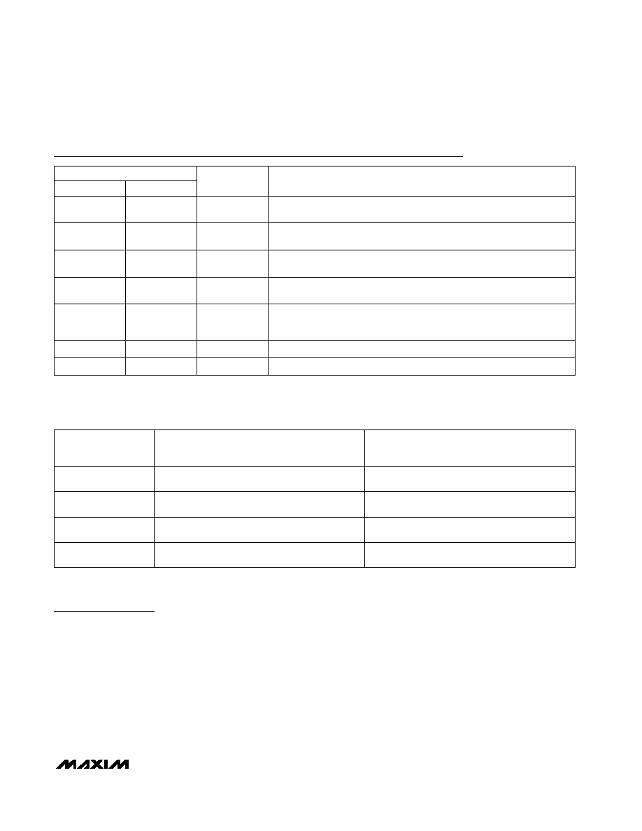
Pin Description
Table 1. Output Matching Components
1.2nH
Murata LQG11AINZS00
2400
1pF
Murata GRM39COG1R0B50V
2.2nH
Murata LQG11AZN2500
1900
1pF
Murata GRM39COG1R0B50V
1pF
Murata GRM39COG1R0B50V
1.5pF
Murata GRM39COG1R5B50V
CMATCH
12nH
Coilcraft 0603HS-12NTJBC
900
22nH
Coilcraft 0603HS-22NTJBC
600
LMATCH
OPERATING
FREQUENCY
(MHz)
FUNCTION
NAME
PIN
MAX2472
MAX2473
—
Open-Collector Buffer Output 1. Connect to VCC via a resistor or
inductor/choke. AC-coupling to the output is required.
—
1
Open-Collector Buffer Output. Connect to VCC via a resistor or
inductor/choke. AC-coupling to the output is required.
2, 5
RF Ground. Connect to the ground plane as close to the IC as possible to
minimize trace inductance.
1
3
—
Open-Collector Buffer Output 2. Connect to VCC via a resistor or
inductor/choke. AC-coupling to the output is required.
—
3
Bias Resistor Connection. Connect a resistor from BIAS to GND to set the
output stage bias current and gain. To choose RBIAS, refer to the Typical
Operating Characteristics for the MAX2473.
6
Supply Voltage Input: +2.7V < VCC < +5.5V
4
High-Impedance Input to the Buffer Amplifier
OUT1
OUT
GND
OUT2
BIAS
VCC
IN
相关PDF资料 |
PDF描述 |
|---|---|
| MAX2471EVKIT | EVAL KIT MAX2470, MAX2471 |
| MAX2470EVKIT | EVAL KIT MAX2470, MAX2471 |
| MAX2654EVKIT | EVAL KIT |
| MAX2208EVKIT | EVAL KIT MAX2208 |
| MAX2657EVKIT+ | KIT EVALUATION FOR MAX2657 |
相关代理商/技术参数 |
参数描述 |
|---|---|
| MAX247CPL | 功能描述:RS-232接口集成电路 RoHS:否 制造商:Exar 数据速率:52 Mbps 工作电源电压:5 V 电源电流:300 mA 工作温度范围:- 40 C to + 85 C 安装风格:SMD/SMT 封装 / 箱体:LQFP-100 封装: |
| MAX247EPL | 功能描述:RS-232接口集成电路 RoHS:否 制造商:Exar 数据速率:52 Mbps 工作电源电压:5 V 电源电流:300 mA 工作温度范围:- 40 C to + 85 C 安装风格:SMD/SMT 封装 / 箱体:LQFP-100 封装: |
| MAX248C/D | 功能描述:RS-232接口集成电路 RoHS:否 制造商:Exar 数据速率:52 Mbps 工作电源电压:5 V 电源电流:300 mA 工作温度范围:- 40 C to + 85 C 安装风格:SMD/SMT 封装 / 箱体:LQFP-100 封装: |
| MAX248C/D DIE | 制造商:Maxim Integrated Products 功能描述: |
| MAX248CQH+D | 功能描述:RS-232接口集成电路 5V MultiCh RS-232 Driver/Receiver RoHS:否 制造商:Exar 数据速率:52 Mbps 工作电源电压:5 V 电源电流:300 mA 工作温度范围:- 40 C to + 85 C 安装风格:SMD/SMT 封装 / 箱体:LQFP-100 封装: |
发布紧急采购,3分钟左右您将得到回复。