- 您现在的位置:买卖IC网 > Datasheet目录473 > MAX2666EVKIT+ (Maxim Integrated)EVAL KIT MAX2666 Datasheet资料下载
参数资料
| 型号: | MAX2666EVKIT+ |
| 厂商: | Maxim Integrated |
| 文件页数: | 7/9页 |
| 文件大小: | 0K |
| 描述: | EVAL KIT MAX2666 |
| 标准包装: | 1 |
| 系列: | * |
�� �
�
�Tiny� Low-Noise� Amplifiers� for� HSPA/LTE�
�Detailed� Description�
�The� MAX2666/MAX2668� are� low-power� LNAs� designed�
�for� 3G� mobile� applications.� The� devices� feature� low�
�noise,� high� linearity,� and� three� gain� steps� in� a� tiny� plastic�
�package.�
�Input� and� Output� Matching�
�The� devices� require� one� matching� inductor� at� the� input�
�port� in� series� with� a� DC-blocking� capacitor� to� achieve�
�optimal� performance� in� NF,� gain,� IIP3,� and� phase� shift.�
�Table� 1� presents� the� recommended� input-matching�
�network� values.� The� output� port� is� internally� matched� to�
�50� I� ,� eliminating� the� need� for� external� matching� com-�
�ponents.� At� the� output� port,� an� external� DC-blocking�
�capacitor� should� be� used� to� isolate� the� control� function�
�of� the� output� pin.�
�DC� Decoupling� and� Layout�
�A� properly� designed� PCB� is� essential� to� any� RF� micro-�
�wave� circuit.� Use� controlled-impedance� lines� on� all�
�high-frequency� inputs� and� outputs.� Bypass� V� CC� with� a�
�decoupling� capacitor� located� close� to� the� device.�
�For� long� V� CC� lines,� it� might� be� necessary� to� add� decou-�
�pling� capacitors.� Locate� these� additional� capacitors�
�further� away� from� the� device� package.� Proper� grounding�
�of� the� GND� pins� is� essential.� If� the� PCB� uses� a� top-side�
�RF� ground,� connect� it� directly� to� the� GND� pins.� For� a�
�board� where� the� ground� is� not� on� the� component� layer,�
�connect� the� GND� pins� to� the� board� with� multiple� vias�
�close� to� the� package.�
�Gain� Control�
�The� devices’� LNA_OUT/GAIN0� pin� is� also� used� as� a�
�control� pin� for� the� LNA� gain� modes� according� to� the� gain�
�control� table.� GAIN0� logic� level� is� set� through� an� external�
�20k� I� resistor.� An� external� DC-blocking� capacitor� should�
�be� used� to� isolate� the� control� function� of� this� dual-pur-�
�pose� pin� (see� the� Typical� Operating� Circuit� ).� The� GAIN1�
�pin� must� be� set� to� either� logic-high� or� logic-low.�
�Refer� to� www.maxim-ic.com� for� the� MAX2666/MAX2668�
�Evaluation� Kit� schematic,� Gerber� data,� PADS� layout� file,�
�and� BOM� information.�
�Table� 1.� Matching� Component� Values� in�
�Different� Bands�
�BAND� SERIES� C� (nF)� SERIES� L� (nH)�
�1,� 4,� 10� 10� 3.9�
�5,� 6� 10� 12�
�8� 10� 12�
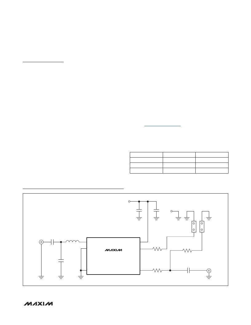
�Detailed� Application� Circuit� in� EV� Kit�
�V� CC�
�C1�
�C5�
�0.01μF�
�10%�
�(0402)�
�1000pF�
�10%�
�(0402)�
�GND�
�1�
�RFIN�
�C4�
�0.01μF�
�10%�
�(0201)�
�C7�
�OPEN�
�(0201)�
�L4�
�3.9nH� Q� 0.1nH� (MAX2666)�
�12nH� Q� 0.2nH� (MAX2668)�
�(0402)�
�2�
�3�
�LNA_IN�
�BIAS_GND�
�LNA_GND�
�U1�
�MAX2666�
�MAX2668�
�V� CC�
�GAIN1�
�LNA_OUT/GAIN0�
�6�
�5�
�4�
�R1�
�0� I�
�(0201)�
�R2�
�0� I�
�(0201)�
�GAIN1�
�R4�
�20k� I�
�(0201)�
�C3�
�0.01μF�
�10%�
�(0201)�
�GAIN0�
�RFOUT�
�_______________________________________________________________________________________�
�7�
�相关PDF资料 |
PDF描述 |
|---|---|
| MAX2669EVKIT+ | KIT EVALUATION FOR MAX2669 |
| MAX2670GTB+TW | IC FRONT-END AMP GPS/GNSS 10TDFN |
| MAX2673EVKIT | EVAL KIT MAX2673 |
| MAX2676EVKIT+ | EVAL KIT MAX2676 |
| MAX2681EVKIT | EVAL KIT |
相关代理商/技术参数 |
参数描述 |
|---|---|
| MAX2666EVKIT+ | 功能描述:放大器 IC 开发工具 MAX2666 Eval Kit RoHS:否 制造商:International Rectifier 产品:Demonstration Boards 类型:Power Amplifiers 工具用于评估:IR4302 工作电源电压:13 V to 23 V |
| MAX2666EYT+ | 功能描述:射频放大器 Ultra Thin HSPA/LTE LNA RoHS:否 制造商:Skyworks Solutions, Inc. 类型:Low Noise Amplifier 工作频率:2.3 GHz to 2.8 GHz P1dB:18.5 dBm 输出截获点:37.5 dBm 功率增益类型:32 dB 噪声系数:0.85 dB 工作电源电压:5 V 电源电流:125 mA 测试频率:2.6 GHz 最大工作温度:+ 85 C 安装风格:SMD/SMT 封装 / 箱体:QFN-16 封装:Reel |
| MAX2666EYT+T | 功能描述:射频放大器 Ultra Thin HSPA/LTE LNA RoHS:否 制造商:Skyworks Solutions, Inc. 类型:Low Noise Amplifier 工作频率:2.3 GHz to 2.8 GHz P1dB:18.5 dBm 输出截获点:37.5 dBm 功率增益类型:32 dB 噪声系数:0.85 dB 工作电源电压:5 V 电源电流:125 mA 测试频率:2.6 GHz 最大工作温度:+ 85 C 安装风格:SMD/SMT 封装 / 箱体:QFN-16 封装:Reel |
| MAX2667EVKIT+ | 功能描述:放大器 IC 开发工具 MAX2667 Eval Kit RoHS:否 制造商:International Rectifier 产品:Demonstration Boards 类型:Power Amplifiers 工具用于评估:IR4302 工作电源电压:13 V to 23 V |
| MAX2667EWT+ | 制造商:Maxim Integrated Products 功能描述:ULTRA LOW NOISE FIGURE GPS/GNSS AMPLIFIER - Rail/Tube |
发布紧急采购,3分钟左右您将得到回复。