- 您现在的位置:买卖IC网 > PDF目录18758 > MAX2669EWT+T10 (Maxim Integrated)IC AMP LNA GPS/GNSS 6-WLP PDF资料下载
参数资料
| 型号: | MAX2669EWT+T10 |
| 厂商: | Maxim Integrated |
| 文件页数: | 6/9页 |
| 文件大小: | 0K |
| 描述: | IC AMP LNA GPS/GNSS 6-WLP |
| 产品培训模块: | Lead (SnPb) Finish for COTS Obsolescence Mitigation Program |
| 标准包装: | 10,000 |
| 频率: | 1575.42MHz |
| P1dB: | -10dBm(0.1mW) |
| 增益: | 17.7dB |
| 噪音数据: | 0.65dB |
| RF 型: | GPS/GNSS |
| 电源电压: | 1.6 V ~ 3.3 V |
| 电流 - 电源: | 7.7mA |
| 测试频率: | 1575.42MHz |
| 封装/外壳: | 6-WFBGA,WLPBGA |
| 包装: | 带卷 (TR) |
�� �
�
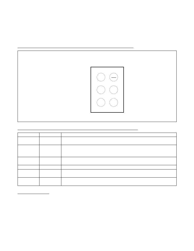
�MAX2667/MAX2669�
�GPS/GNSS� Ultra-Low-Noise-Figure� LNAs�
�Bump� Configuration�
�TOP� VIEW�
�BUMP� SIDE� DOWN�
�MAX2667/MAX2669�
�+�
�1�
�2�
�A�
�B�
�C�
�BIAS�
�RFIN�
�GNDAC�
�WLP�
�R� FOUT� /�
�SHDN�
�V� CC�
�GNDDC�
�Bump� Description�
�BUMP�
�A1�
�A2�
�B1�
�B2�
�C1�
�C2�
�NAME�
�BIAS�
�RFOUT/� SHDN�
�RFIN�
�V� CC�
�GNDAC�
�GNDDC�
�FUNCTION�
�Provides� Bias� for� LNA� Input.� Connect� to� B1� (RFIN)� through� a� high-value� inductor� (100nH),�
�and� bypass� to� ground� close� to� the� pin.�
�RF� Output� and� SHDN� Logic� Input.� RFOUT� is� internally� matched� to� 50� I� and� has� an� internal�
�DC-blocking� capacitor.� The� SHDN� logic� requires� an� external� 25k� ?� resistor� to� the� logic�
�control.�
�RF� Input.� Connect� to� A1� through� bias� choke,� and� connect� matching� network� and�
�DC-blocking� capacitor.�
�Supply� Voltage.� Bypass� to� ground� with� a� capacitor� close� to� the� IC.�
�Ground� of� the� RF� Path.� Connect� to� the� 2nd-layer� PCB� ground� plane� with� a� via� next� to� the�
�pin� pad.�
�Ground� of� Bias� Circuit.� Connect� to� the� 2nd-layer� PCB� ground� plane� with� a� separate� via�
�from� pin� C1.� Sharing� a� ground� via� with� pin� C1� might� cause� stability� problems.�
�Detailed� Description�
�The� MAX2667/MAX2669� are� LNAs� designed� for� GPS�
�L1,� Galileo,� and� GLONASS� applications.� The� devices�
�feature� a� power-shutdown� control� mode� to� eliminate� the�
�need� for� an� external� supply� switch.� The� devices� achieve�
�a� high� gain� and� an� ultra-low� noise� figure.�
�Input� and� Output� Matching�
�The� devices� require� an� off-chip� input� matching.� Only�
�an� inductor� in� series� with� a� DC-blocking� capacitor� is�
�6�
�needed� to� form� the� input� matching� circuit.� The� Typical�
�Application� Circuit� shows� the� recommended� input-�
�matching� network.� These� values� are� optimized� for� the�
�best� simultaneous� gain,� noise� figure,� and� return� loss�
�performance.� Tables� 1� and� 2� list� typical� device� S� param-�
�eters� and� K� f� values.� The� devices� integrate� an� on-chip�
�output� matching� to� 50Ω� at� the� output,� eliminating� the�
�need� for� external� matching� components.� The� value� of� the�
�input� coupling� capacitor� affects� IIP3.� A� smaller� coupling�
�capacitor� results� in� lower� IIP3.�
�Maxim� Integrated�
�相关PDF资料 |
PDF描述 |
|---|---|
| MAX2667EWT+T10 | IC AMP LNA GPS/GNSS 6-WLP |
| DP-241-6-36L | XFRMR PWR 115/230V 36VCT 0.85A |
| MAX2695EWS+T | IC RF LNA WLAN/WIMAX 4WLP |
| DP-241-6-28L | XFRMR PWR 115/230V 28VCT 1.1A |
| FI105B245024-T | FILTER BANDPASS 2.5GHZ SMD |
相关代理商/技术参数 |
参数描述 |
|---|---|
| MAX266ACPI | 功能描述:有源滤波器 RoHS:否 制造商:Maxim Integrated 通道数量:1 截止频率:150 KHz 电源电压-最大:11 V 电源电压-最小:4.74 V 最大工作温度:+ 85 C 安装风格:Through Hole 封装 / 箱体:PDIP N 封装:Tube |
| MAX266ACPI+ | 功能描述:有源滤波器 Integrated Circuits (ICs) RoHS:否 制造商:Maxim Integrated 通道数量:1 截止频率:150 KHz 电源电压-最大:11 V 电源电压-最小:4.74 V 最大工作温度:+ 85 C 安装风格:Through Hole 封装 / 箱体:PDIP N 封装:Tube |
| MAX266ACWI | 功能描述:有源滤波器 RoHS:否 制造商:Maxim Integrated 通道数量:1 截止频率:150 KHz 电源电压-最大:11 V 电源电压-最小:4.74 V 最大工作温度:+ 85 C 安装风格:Through Hole 封装 / 箱体:PDIP N 封装:Tube |
| MAX266ACWI+ | 功能描述:有源滤波器 Integrated Circuits (ICs) RoHS:否 制造商:Maxim Integrated 通道数量:1 截止频率:150 KHz 电源电压-最大:11 V 电源电压-最小:4.74 V 最大工作温度:+ 85 C 安装风格:Through Hole 封装 / 箱体:PDIP N 封装:Tube |
| MAX266ACWI+T | 功能描述:有源滤波器 Integrated Circuits (ICs) RoHS:否 制造商:Maxim Integrated 通道数量:1 截止频率:150 KHz 电源电压-最大:11 V 电源电压-最小:4.74 V 最大工作温度:+ 85 C 安装风格:Through Hole 封装 / 箱体:PDIP N 封装:Tube |
发布紧急采购,3分钟左右您将得到回复。