- 您现在的位置:买卖IC网 > PDF目录18816 > MAX2670GTB+T (Maxim Integrated)IC AMP GPS/GNSS FRONTEND 10TDFN PDF资料下载
参数资料
| 型号: | MAX2670GTB+T |
| 厂商: | Maxim Integrated |
| 文件页数: | 7/9页 |
| 文件大小: | 0K |
| 描述: | IC AMP GPS/GNSS FRONTEND 10TDFN |
| 产品培训模块: | Lead (SnPb) Finish for COTS Obsolescence Mitigation Program |
| 标准包装: | 1 |
| RF 型: | GPS/GNSS |
| 频率: | 1575MHz |
| 封装/外壳: | 10-WFDFN 裸露焊盘 |
| 供应商设备封装: | 10-TDFN-EP(3x3) |
| 包装: | 标准包装 |
| 其它名称: | MAX2670GTB+TDKR |
�� �
�
�MAX2670�
�GPS/GNSS� Front-End� Amplifier�
�Detailed� Description�
�The� MAX2670� IC� contains� two� LNA� stages� tuned� for� use�
�at� 1575MHz.�
�AMP� 1�
�AMP� 1� has� an� internal� load� that� limits� the� bandwidth� and�
�provides� a� 50� I� output� impedance� through� a� DC-blocking�
�capacitor.� The� internal� biasing� for� AMP� 1� suppresses�
�gain� variation� with� changes� in� temperature� and� supply�
�voltage.� At� the� input,� an� integrated� DC-blocking� capaci-�
�tor� and� matching� network� are� intentionally� omitted� to�
�allow� selection� of� external� components� to� optimize� for�
�noise� or� gain.�
�AMP� 2� with� Gain� Step�
�The� output� of� AMP� 2� has� the� dual� role� of� providing� both�
�the� RF� output� drive� and� receiving� the� DC� power� supply�
�through� a� single� cable.� Both� the� input� and� output� ports�
�of� AMP� 2� are� internally� matched� to� 50� I� impedance� at�
�1575MHz.� A� 3.4dB� gain� switch� can� be� used� to� adjust�
�the� gain� for� different� applications.� The� gain-select� pin� is�
�connected� to� an� inverter� with� an� internal� pullup� resistor.�
�Hence,� the� gain-select� pin� is� set� by� default� to� high-gain�
�mode.� Shorting� the� gain-select� pin� to� ground� sets� the�
�gain� stage� to� a� 3.4dB� lower� gain.� As� with� AMP� 1,� AMP�
�Alternate� Supply� (ALT_VCC)�
�The� IC� power� can� be� supplied� from� the� navigation� sys-�
�tem� through� RFOUT2� (pin� 5).� An� integrated� filter� is� con-�
�nected� to� the� output� of� LNA� 2� to� separate� the� supply� volt-�
�age� from� the� GPS� signal.� Alternatively,� the� supply� voltage�
�can� be� applied� to� the� external� capacitor� pin� (pin� 4).�
�Layout� Considerations�
�For� best� performance,� carefully� lay� out� the� PCB� using�
�high-frequency� techniques.� Use� controlled-impedance�
�transmission� lines� to� interface� with� the� MAX2670� high-�
�speed� inputs� and� outputs� and� isolate� the� input� sig-�
�nals� from� the� output� signals� as� much� as� possible.� For�
�improved� noise� figure,� keep� the� connection� to� the� input�
�of� LNA� 1� as� short� as� possible.� A� power-supply� decou-�
�pling� capacitor� should� be� placed� very� close� to� pin� 4� and�
�connected� directly� to� a� ground� plane.� If� low-gain� selec-�
�tion� for� LNA� 2� is� required,� connect� pin� 7� directly� to� the�
�ground� plane� with� a� very� short� PCB� trace.� Good� ground-�
�ing� is� critical� for� this� device.� The� backside� ground� plane�
�should� be� as� close� as� possible.�
�Refer� to� www.maxim-ic.com� for� the� MAX2670� Evaluation�
�Kit� schematic,� gerber� data,� pads� layout� file� and� BOM�
�information.�
�2� has� an� internal� load� that� limits� the� bandwidth,� and� the�
�amplifier’s� internal� biasing� suppresses� gain� variation� with�
�changes� in� temperature� and� supply� voltage.�
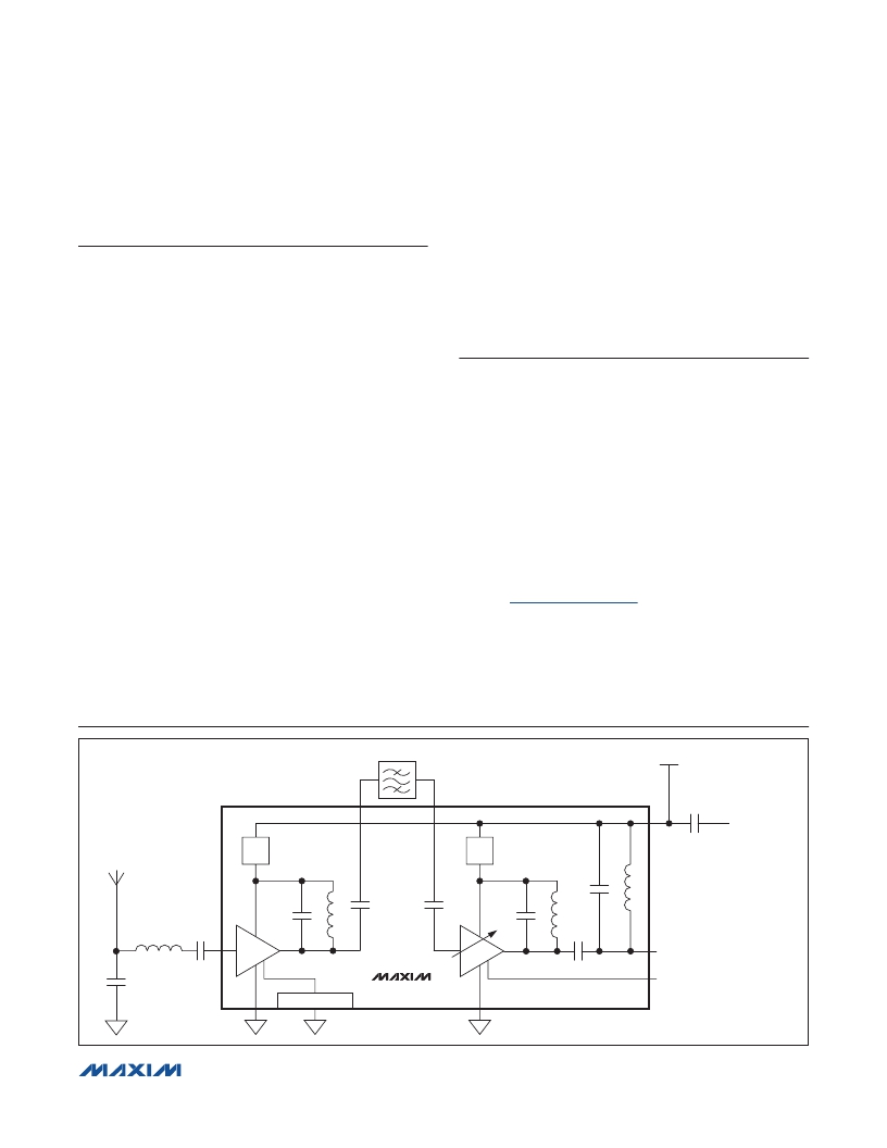
�Typical� Operating� Circuit�
�LNA1� INPUT�
�SAW�
�LNA2� INPUT�
�ALT_VCC�
�V� CC�
�REG�
�10�
�1�
�V� CC�
�REG�
�4�
�6�
�LNA� 1�
�LNA� 2�
�5�
�RFOUT2/VCC�
�8/9�
�EXPOSED� PAD�
�MAX2670�
�2/3�
�7�
�GAIN_SELECT�
�OPEN� =� 31.4dB� GAIN�
�SHORT� TO� GROUND� =� 28dB� GAIN�
�?????????????????????????????????????????????????????????????????� Maxim� Integrated� Products� 7�
�相关PDF资料 |
PDF描述 |
|---|---|
| 7C-4.000MBA-T | OSC 4.000 MHZ 3.3V SMT |
| 633W-60 VLT | LEAD TEST MINIHK-RA BANAPLG VLT |
| BU52002GUL-E2 | IC HALL EFFECT SW BIPO VCSP50L1 |
| D75J-038.88M | OSC TCXO 38.880 MHZ 3.3V SMD |
| TA20041803DH | SCR PHASE CTRL 400V 1800A |
相关代理商/技术参数 |
参数描述 |
|---|---|
| MAX2671EUT | 制造商:Maxim Integrated Products 功能描述:- Rail/Tube 制造商:Rochester Electronics LLC 功能描述: |
| MAX2671EUT+ | 制造商:Maxim Integrated Products 功能描述:UP/DOWN CONV MIXER 3.3V/5V 2.5GHZ 6PIN SOT-23 - Rail/Tube 制造商:Maxim Integrated Products 功能描述:Mixer/Upconv, 0.4-2.5GHz, MAX2671EUT+ |
| MAX2671EUT+T | 功能描述:上下转换器 400MHz to 2.5GHz Upconverter RoHS:否 制造商:Texas Instruments 产品:Down Converters 射频:52 MHz to 78 MHz 中频:300 MHz LO频率: 功率增益: P1dB: 工作电源电压:1.8 V, 3.3 V 工作电源电流:120 mA 最大功率耗散:1 W 最大工作温度:+ 85 C 安装风格:SMD/SMT 封装 / 箱体:PQFP-128 |
| MAX2671EUT-T | 功能描述:上下转换器 400MHz to 2.5GHz Upconverter RoHS:否 制造商:Texas Instruments 产品:Down Converters 射频:52 MHz to 78 MHz 中频:300 MHz LO频率: 功率增益: P1dB: 工作电源电压:1.8 V, 3.3 V 工作电源电流:120 mA 最大功率耗散:1 W 最大工作温度:+ 85 C 安装风格:SMD/SMT 封装 / 箱体:PQFP-128 |
| MAX2671EUT-T+ | 制造商:Maxim Integrated Products 功能描述:Upconverter Mixer,MAX2671 400-2500MHz |
发布紧急采购,3分钟左右您将得到回复。