- 您现在的位置:买卖IC网 > PDF目录18721 > MAX2674EWT+T (Maxim Integrated)RF AMP GPS GNSS LNA 6WLP PDF资料下载
参数资料
| 型号: | MAX2674EWT+T |
| 厂商: | Maxim Integrated |
| 文件页数: | 7/9页 |
| 文件大小: | 0K |
| 描述: | RF AMP GPS GNSS LNA 6WLP |
| 标准包装: | 1 |
| 频率: | 1575.42MHz |
| 增益: | 18dB |
| 噪音数据: | 0.75dB |
| RF 型: | GPS/GNSS |
| 电源电压: | 1.6 V ~ 3.6 V |
| 电流 - 电源: | 7mA |
| 测试频率: | 1575.42MHz |
| 封装/外壳: | 6-WFBGA,WLPBGA |
| 包装: | 标准包装 |
| 其它名称: | MAX2674EWT+TDKR |
�� �
�
�GPS/GNSS� LNAs� with� Antenna� Switch� and� Bias�
�Detailed� Description�
�The� MAX2674/MAX2676� are� low-power� LNAs� designed�
�for� GPS/GNSS� receiver� applications.� The� devices� feature�
�low� noise� and� high� linearity� in� an� ultra-small� package.�
�They� also� include� an� antenna� switch� and� circuitry� sup-�
�porting� bias� to� accommodate� external� LNA� applications.�
�Input� and� Output� Matching�
�To� achieve� optimal� performance� in� noise� figure,� gain,�
�and� IIP3,� the� devices� require� one� matching� inductor� at�
�RFIN� in� series� with� a� DC-blocking� capacitor.� RFOUT/�
�SHDN� is� internally� matched� to� 50� I� ,� eliminating� the� need�
�for� external� matching� components.� At� RFOUT/� SHDN� ,� an�
�external� DC-blocking� capacitor� should� be� used� to� isolate�
�the� shutdown� control� function.�
�Shutdown� Mode�
�To� place� the� device� in� shutdown� mode,� apply� logic-low�
�to� RFOUT/� SHDN� through� a� 25k?� resistor.� An� additional�
�DC-blocking� capacitor� or� component� is� required� at�
�RFOUT/� SHDN� in� this� case.� Apply� a� logic-high� state� or� no�
�DC� bias� to� turn� the� part� permanently� on.�
�DC� Supply� Decoupling� and� Layout�
�A� properly� designed� PC� board� (PCB)� is� essential� to� any�
�RF� microwave� circuit.� Use� controlled-impedance� lines�
�on� all� high-frequency� inputs� and� outputs.� Bypass� V� CC�
�with� a� decoupling� capacitor� located� close� to� the� device.�
�For� long� V� CC� lines,� it� may� be� necessary� to� add� additional�
�decoupling� capacitors.� Locate� these� additional� capaci-�
�tors� further� away� from� the� device� package.�
�Proper� grounding� of� GND_� pins� is� essential.� If� the� PCB�
�uses� a� top-side� RF� ground,� connect� it� directly� to� the�
�GND_� pins.� For� a� board� where� the� ground� is� not� on� the�
�component� layer,� connect� the� GND_� pins� to� the� board�
�with� multiple� vias� close� to� the� package.�
�Antenna� Switch� Control�
�The� MAX2674/MAX2676� ANT� input� includes� an� autode-�
�tection� feature.� When� no� current� is� drawn� from� ANT,� the�
�switch� defaults� to� normal� LNA� operation.� The� pin� can� be�
�directly� connected� to� an� external� active� antenna.� The�
�device� automatically� switches� to� the� ANT� input� when� an�
�external� active� antenna� is� connected.�
�Refer� to� www.maxim-ic.com� for� the� MAX2674/MAX2676�
�EV� Kit� schematic,� layout� files,� BOM� information,� and�
�S-parameters.�
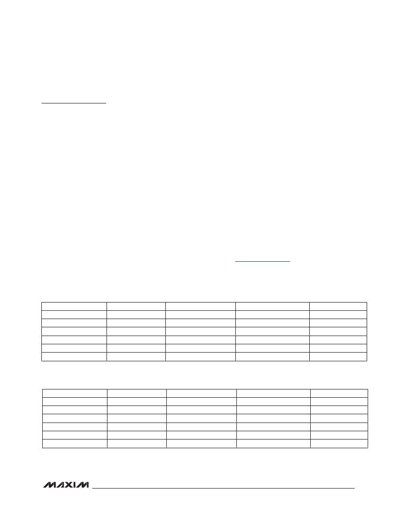
�Table 1. MAX267� 4� Typical� Noise� Parameters� (V� CC� =� 2.85V,� T� A� =� +25°C)�
�FREQUENCY� (MHz)�
�1550�
�1560�
�1570�
�1580�
�1590�
�1600�
�NF� MIN� (dB)�
�0.651�
�0.652�
�0.654�
�0.655�
�0.656�
�0.657�
�GAMMA_OPT� MAG� (� °� )�
�0.446�
�0.445�
�0.445�
�0.444�
�0.444�
�0.443�
�GAMMA_OPT� PHASE� (� °� )�
�44.1�
�44.3�
�44.6�
�44.8�
�45.1�
�45.4�
�Rn� (� I� )�
�8.33�
�8.33�
�8.32�
�8.31�
�8.3�
�8.3�
�Table 2. MAX2676� Typical� Noise� Parameters� (V� CC� =� 2.85V,� T� A� =� +25°C)�
�FREQUENCY� (MHz)�
�1550�
�1560�
�1570�
�1580�
�1590�
�1600�
�NF� MIN� (dB)�
�0.744�
�0.746�
�0.748�
�0.75�
�0.751�
�0.753�
�GAMMA_OPT� MAG� (� °� )�
�0.441�
�0.44�
�0.439�
�0.438�
�0.437�
�0.436�
�GAMMA_OPT� PHASE� (� °� )�
�53.1�
�53.4�
�53.7�
�54�
�54.3�
�54.7�
�Rn� (� I� )�
�8.7�
�8.68�
�8.66�
�8.65�
�8.63�
�8.62�
�7�
�相关PDF资料 |
PDF描述 |
|---|---|
| SG923-0012-5.0-C | RF EVAL WI-FI MODULE |
| PM113-161.1328M | OSC 161.1328 MHZ 3.3V LVPECL |
| SG923-0012-3.3-H | RF EVAL WI-FI MODULE |
| MAX2640EUT+T | IC AMPLIFIER ULTRA-LN SOT23-6 |
| HM31-20200LLF | ENCAPSULATED CURRENT SENSE TRANS |
相关代理商/技术参数 |
参数描述 |
|---|---|
| MAX2675EWT+T | 功能描述:射频放大器 GPS LNA w/antenna bypass switch RoHS:否 制造商:Skyworks Solutions, Inc. 类型:Low Noise Amplifier 工作频率:2.3 GHz to 2.8 GHz P1dB:18.5 dBm 输出截获点:37.5 dBm 功率增益类型:32 dB 噪声系数:0.85 dB 工作电源电压:5 V 电源电流:125 mA 测试频率:2.6 GHz 最大工作温度:+ 85 C 安装风格:SMD/SMT 封装 / 箱体:QFN-16 封装:Reel |
| MAX2675EWT+T10 | 功能描述:射频放大器 GPS LNA w/antenna bypass switch RoHS:否 制造商:Skyworks Solutions, Inc. 类型:Low Noise Amplifier 工作频率:2.3 GHz to 2.8 GHz P1dB:18.5 dBm 输出截获点:37.5 dBm 功率增益类型:32 dB 噪声系数:0.85 dB 工作电源电压:5 V 电源电流:125 mA 测试频率:2.6 GHz 最大工作温度:+ 85 C 安装风格:SMD/SMT 封装 / 箱体:QFN-16 封装:Reel |
| MAX2676EVKIT+ | 功能描述:放大器 IC 开发工具 MAX2676 Eval Kit RoHS:否 制造商:International Rectifier 产品:Demonstration Boards 类型:Power Amplifiers 工具用于评估:IR4302 工作电源电压:13 V to 23 V |
| MAX2676EWT+ | 制造商:Maxim Integrated Products 功能描述:- Rail/Tube |
| MAX2676EWT+T | 功能描述:射频放大器 GPS LNA w/antenna Bypass Switch RoHS:否 制造商:Skyworks Solutions, Inc. 类型:Low Noise Amplifier 工作频率:2.3 GHz to 2.8 GHz P1dB:18.5 dBm 输出截获点:37.5 dBm 功率增益类型:32 dB 噪声系数:0.85 dB 工作电源电压:5 V 电源电流:125 mA 测试频率:2.6 GHz 最大工作温度:+ 85 C 安装风格:SMD/SMT 封装 / 箱体:QFN-16 封装:Reel |
发布紧急采购,3分钟左右您将得到回复。