- 您现在的位置:买卖IC网 > PDF目录18745 > MAX2688LEWS+T (Maxim Integrated)IC LNA GPS/GNSS 4WLP PDF资料下载
参数资料
| 型号: | MAX2688LEWS+T |
| 厂商: | Maxim Integrated |
| 文件页数: | 5/8页 |
| 文件大小: | 0K |
| 描述: | IC LNA GPS/GNSS 4WLP |
| 标准包装: | 2,500 |
| 频率: | 1575.42MHz |
| P1dB: | -10dBm(0.1mW) |
| 增益: | 15.4dB |
| 噪音数据: | 0.75dB |
| RF 型: | GPS/GNSS |
| 电源电压: | 1.6 V ~ 3.3 V |
| 电流 - 电源: | 4.1mA |
| 测试频率: | 1575.42MHz |
| 封装/外壳: | 4-WFBGA,WLCSP |
| 包装: | 带卷 (TR) |
�� �
�
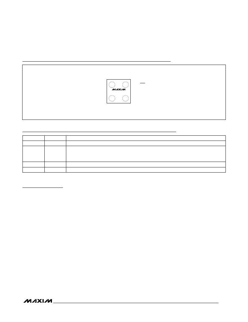
�GPS/GNSS� Low-Noise� Amplifiers�
�Bump� Configuration�
�TOP� VIEW�
�+�
�V� CC�
�A1�
�A2�
�RFOUT� (SHDN)�
�MAX2686�
�MAX2688�
�RFIN�
�B1�
�B2�
�GND�
�WLP�
�Bump� Description�
�BUMP�
�A1�
�A2�
�B1�
�B2�
�NAME�
�V� CC�
�RFOUT�
�(� SHDN� )�
�RFIN�
�GND�
�FUNCTION�
�Supply� Voltage.� Bypass� to� ground� with� a� 10pF� capacitor� as� close� as� possible� to� the� IC.�
�RF� Output/� SHDN� Input.� RFOUT� is� internally� matched� to� 50� I� and� pulled� up� to� V� CC� through� a� 1M� I�
�resistor.� SHDN� is� shared� with� the� RFOUT� bump.� The� devices� are� in� active� mode� by� default� once�
�V� CC� is� applied.� RFOUT(� SHDN� )� can� be� pulled� to� a� DC� low� externally� to� shut� down� the� IC.�
�RF� Input.� Requires� a� DC-blocking� capacitor� and� external� matching� components.�
�Ground.� Connect� to� the� PCB� ground� plane.�
�Detailed� Description�
�The� MAX2686/MAX2688� are� LNAs� designed� for� GPS�
�L1,� Galileo,� and� GLONASS� applications.� The� devices�
�feature� an� optional� power-shutdown� control� mode� to�
�eliminate� the� need� for� an� external� supply� switch.� The�
�devices� achieve� high� gain,� ultra-low-noise� figure,� and�
�excellent� linearity.�
�Input� and� Output� Matching�
�The� devices� require� an� off-chip� input� matching.� Only�
�an� inductor� in� series� with� a� DC-blocking� capacitor� is�
�needed� to� form� the� input� matching� circuit.� The� Typical�
�Application� Circuit� shows� the� recommended� input-�
�matching� network.� These� values� are� optimized� for� the�
�best� simultaneous� gain,� noise� figure,� and� return� loss�
�performance.� The� value� of� the� input� coupling� capacitor�
�affects� IIP3.� A� smaller� coupling� capacitor� results� in� lower�
�IIP3.� The� devices� integrate� an� on-chip� output� matching�
�to� 50� I� at� the� output,� eliminating� the� need� for� external�
�matching� components.� Tables� 1� and� 2� list� typical� device�
�S� parameters� and� K� f� values.� Typical� noise� parameters�
�are� shown� in� Tables� 3� and� 4.�
�Shutdown�
�The� devices� include� an� optional� shutdown� feature� to�
�turn� off� the� entire� chip.� The� devices� are� placed� in� active�
�mode� by� default� once� V� CC� is� applied,� due� to� the� on-chip�
�pullup� resistor� to� V� CC� at� the� RFOUT� bump� (shared� with�
�the� SHDN� input).� To� shut� down� the� part,� apply� a� logic-�
�low� to� the� RFOUT� bump� through� an� external� resistor� with�
�an� adequate� value,� e.g.,� 25k� I� ,� in� order� not� to� load� the�
�RF� output� signal� during� active� operation.�
�5�
�相关PDF资料 |
PDF描述 |
|---|---|
| MAX2691LEWS+T | IC LNA GPS/GNSS 4WLP |
| MAX2691EWS+T | IC LNA GPS/GNSS 4WLP |
| GLCB01A1B | SWITCH SIDE-ROTRY ROLL SNAP SPDT |
| NDP6060 | MOSFET N-CH 60V 48A TO-220AB |
| 56-1 | XFRMR PWR 115V 56VCT 1A |
相关代理商/技术参数 |
参数描述 |
|---|---|
| MAX2689EWS+T | 功能描述:射频放大器 GPS/GNSS LO-NOISE AMP RoHS:否 制造商:Skyworks Solutions, Inc. 类型:Low Noise Amplifier 工作频率:2.3 GHz to 2.8 GHz P1dB:18.5 dBm 输出截获点:37.5 dBm 功率增益类型:32 dB 噪声系数:0.85 dB 工作电源电压:5 V 电源电流:125 mA 测试频率:2.6 GHz 最大工作温度:+ 85 C 安装风格:SMD/SMT 封装 / 箱体:QFN-16 封装:Reel |
| MAX2689EWS+T10 | 功能描述:射频放大器 GPS/GNSS Low-Noise Amplifier RoHS:否 制造商:Skyworks Solutions, Inc. 类型:Low Noise Amplifier 工作频率:2.3 GHz to 2.8 GHz P1dB:18.5 dBm 输出截获点:37.5 dBm 功率增益类型:32 dB 噪声系数:0.85 dB 工作电源电压:5 V 电源电流:125 mA 测试频率:2.6 GHz 最大工作温度:+ 85 C 安装风格:SMD/SMT 封装 / 箱体:QFN-16 封装:Reel |
| MAX2689LEWS+T | 功能描述:射频放大器 GPS/GNSS Low-Noise Amplifier RoHS:否 制造商:Skyworks Solutions, Inc. 类型:Low Noise Amplifier 工作频率:2.3 GHz to 2.8 GHz P1dB:18.5 dBm 输出截获点:37.5 dBm 功率增益类型:32 dB 噪声系数:0.85 dB 工作电源电压:5 V 电源电流:125 mA 测试频率:2.6 GHz 最大工作温度:+ 85 C 安装风格:SMD/SMT 封装 / 箱体:QFN-16 封装:Reel |
| MAX2689LEWS+T10 | 功能描述:射频放大器 GPS/GNSS Low-Noise Amplifier RoHS:否 制造商:Skyworks Solutions, Inc. 类型:Low Noise Amplifier 工作频率:2.3 GHz to 2.8 GHz P1dB:18.5 dBm 输出截获点:37.5 dBm 功率增益类型:32 dB 噪声系数:0.85 dB 工作电源电压:5 V 电源电流:125 mA 测试频率:2.6 GHz 最大工作温度:+ 85 C 安装风格:SMD/SMT 封装 / 箱体:QFN-16 封装:Reel |
| MAX268ACNG | 功能描述:有源滤波器 RoHS:否 制造商:Maxim Integrated 通道数量:1 截止频率:150 KHz 电源电压-最大:11 V 电源电压-最小:4.74 V 最大工作温度:+ 85 C 安装风格:Through Hole 封装 / 箱体:PDIP N 封装:Tube |
发布紧急采购,3分钟左右您将得到回复。