- 您现在的位置:买卖IC网 > PDF目录18730 > MAX2690EUB+ (Maxim Integrated)IC MIXER DOWNCONVERTER 10UMAX PDF资料下载
参数资料
| 型号: | MAX2690EUB+ |
| 厂商: | Maxim Integrated |
| 文件页数: | 8/10页 |
| 文件大小: | 0K |
| 描述: | IC MIXER DOWNCONVERTER 10UMAX |
| 产品培训模块: | Lead (SnPb) Finish for COTS Obsolescence Mitigation Program |
| 标准包装: | 50 |
| RF 型: | 手机,CDMA,ISM,PCS,WLAN |
| 频率: | 400MHz ~ 2.5GHz |
| 混频器数目: | 1 |
| 增益: | 7.9dB |
| 噪音数据: | 12dB |
| 次要属性: | 降频变频器 |
| 电流 - 电源: | 20.1mA |
| 电源电压: | 2.7 V ~ 5.5 V |
| 包装: | 管件 |
| 封装/外壳: | 10-TFSOP,10-MSOP(0.118",3.00mm 宽) |
| 供应商设备封装: | 10-µMAX |
�� �
�
�Low-Noise,� 2.5GHz�
�Downconverter� Mixer�
�__________Applications� Information�
�Local-Oscillator� (LO)� Input�
�The� LO� input� is� a� single-ended� broadband� 50� ?� input� with�
�a� return� loss� of� better� than� 10dB� from� 900MHz� to� 3GHz,�
�improving� at� high� frequency.� For� lower-frequency� LO�
�operation,� a� shunt� resistor� can� be� used� to� improve� the� LO�
�port� match� (see� the� Typical� Operating� Circuit� for� more�
�information).� AC� couple� to� LO.� The� LO� signal� is� mixed�
�with� the� input� RF� signal,� and� the� resulting� downconverted�
�output� appears� on� the� IFOUT+� and� IFOUT-� pins.�
�RF� Input�
�The� typical� RF� input� frequency� range� is� 400MHz� to�
�2.5GHz.� For� optimum� performance,� the� RF� input� requires�
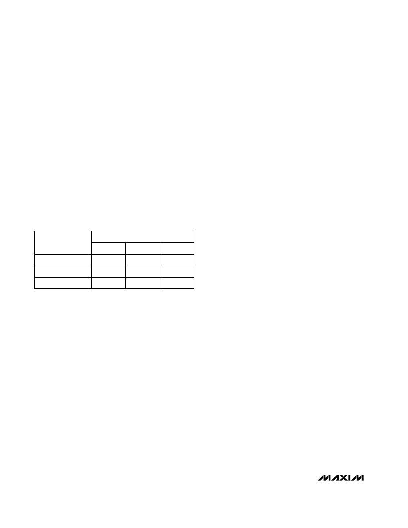
�an� impedance-matching� network.� Consult� Table� 1� as� well�
�as� the� RF� Port� Impedance� vs.� Frequency� graph� in� the�
�Typical� Operating� Characteristics.�
�Table� 1.� RF� Input� Impedance�
�FREQUENCY�
�plane.� Low-inductance� ground� connections� and� con-�
�trolled-impedance� lines� should� be� used� in� the� layout.�
�To� minimize� noise� on� the� internal� bias� cell,� SHDN�
�should� be� decoupled� with� a� 1000pF� capacitor� to�
�ground.� A� series� resistor� (typically� 100� ?� )� can� also� be�
�used� to� reduce� high-frequency� signals� coupling� into�
�the� SHDN� pin.�
�Inductive� Degeneration� Pin� (LGND)�
�A� series� inductor� is� typically� connected� from� LGND� to�
�GND.� Adjusting� the� value� of� this� inductor� allows� the�
�MAX2690� to� be� set� to� the� optimum� gain� and� linearity�
�point� for� a� particular� application.� A� short� from� LGND� to�
�ground� provides� maximum� linearity.� Increasing� the� induc-�
�tor� value� trades� off� linearity� for� gain.� A� large� inductor� pro-�
�vides� maximum� gain.� See� the� Typical� Operating�
�Characteristics� for� a� graph� of� conversion� gain� and� lineari-�
�ty� for� several� inductor� values.� The� inductor’s� self-resonant�
�frequency� (SRF)� should� be� as� close� as� possible� to� or�
�above� the� desired� RF� frequency� for� optimal� performance.�
�______________________Layout� Issues�
�PART�
�Series� Z�
�Equivalent� Shunt� R�
�Equivalent� Shunt� C�
�900MHz�
�45� –� j� 219� ?�
�1100� ?�
�0.7pF�
�1.95GHz�
�20� –� j� 110� ?�
�630� ?�
�0.7pF�
�2.45GHz�
�18� –� j� 85� ?�
�400� ?�
�0.7pF�
�A� well-designed� PC� board� is� an� essential� part� of� an� RF�
�circuit.� For� best� performance,� pay� attention� to� power-�
�supply� issues� as� well� as� the� layout� of� the� RFIN� match-�
�ing� network.�
�Power-Supply� Layout�
�To� minimize� coupling� between� different� sections� of� the�
�IC,� the� ideal� power-supply� layout� is� a� star� configuration,�
�IF� Output�
�The� IF� output� frequency� range� is� typically� 10MHz� to�
�500MHz.� The� IFOUT+� and� IFOUT-� pins� require� external�
�inductors� to� V� CC� for� proper� biasing.� These� outputs� are�
�high-impedance� open� collectors.� In� many� applications,�
�the� biasing� inductors� have� resistors� in� parallel� with�
�them� to� set� an� output� impedance.� Alternatively,� a� resis-�
�tor� between� IFOUT+� and� IFOUT-� may� be� used.� Consult�
�the� Typical� Operating� Characteristics� section� for� more�
�information.�
�For� single-ended� operation,� the� IFOUT-� pin� can� be� tied�
�directly� to� V� CC� .�
�Power� Supply� and� Bypassing�
�Proper� attention� to� supply� bypassing� is� essential� for� a�
�high-frequency� RF� circuit.� V� CC� (pin� 5)� must� be� properly�
�bypassed� with� a� 0.1μF� capacitor� in� parallel� with�
�1000pF� to� ground.� Separate� vias� to� the� ground� plane�
�are� needed� for� each� of� the� bypass� capacitors,� as� well�
�as� minimal� trace� length� to� reduce� inductance.� Each�
�ground� pin� should� have� a� separate� via� to� the� ground�
�which� has� a� large� decoupling� capacitor� at� a� central�
�V� CC� node.� The� V� CC� traces� branch� out� from� this� node,�
�each� going� to� a� separate� V� CC� node� in� the� MAX2690�
�circuit.� At� the� end� of� each� of� these� traces� is� a� bypass�
�capacitor� that� is� good� at� the� RF� frequency� of� interest.�
�This� arrangement� provides� local� decoupling� at� each�
�V� CC� pin.� At� high� frequencies,� any� signal� leaking� out�
�one� supply� pin� sees� a� relatively� high� impedance�
�(formed� by� the� V� CC� trace� inductance)� to� the� central�
�V� CC� node,� and� an� even� higher� impedance� to� any� other�
�supply� pin,� as� well� as� a� low� impedance� to� ground.�
�Matching-Network� Layout�
�The� layout� of� the� RFIN� matching� network� can� be� very�
�sensitive� to� parasitic� circuit� elements.� To� minimize� par-�
�asitic� inductance,� keep� all� traces� short,� and� place� com-�
�ponents� as� close� to� the� chip� as� possible.� To� minimize�
�parasitic� capacitance,� a� cut-out� in� the� ground� plane�
�(and� any� other� planes)� below� the� matching� network�
�components� can� be� used.�
�8�
�_______________________________________________________________________________________�
�相关PDF资料 |
PDF描述 |
|---|---|
| MAX2690EUB+T | IC MIXER DOWNCONVERTER 10UMAX |
| 636L3C011M05920 | OSCILLATOR 11.0592 MHZ 3.3V SMD |
| MAX2685EEE+ | IC MIXER DOWNCONVERTER 16-QSOP |
| MAX2673EUA+ | IC MIXER UPCONVERTER 8-UMAX |
| 0639100170 | TOOL KIT |
相关代理商/技术参数 |
参数描述 |
|---|---|
| MAX2690EUB+ | 功能描述:上下转换器 Low-Noise 2.5GHz Downconverter Mixer RoHS:否 制造商:Texas Instruments 产品:Down Converters 射频:52 MHz to 78 MHz 中频:300 MHz LO频率: 功率增益: P1dB: 工作电源电压:1.8 V, 3.3 V 工作电源电流:120 mA 最大功率耗散:1 W 最大工作温度:+ 85 C 安装风格:SMD/SMT 封装 / 箱体:PQFP-128 |
| MAX2690EUB+T | 功能描述:上下转换器 Low-Noise 2.5GHz Downconverter Mixer RoHS:否 制造商:Texas Instruments 产品:Down Converters 射频:52 MHz to 78 MHz 中频:300 MHz LO频率: 功率增益: P1dB: 工作电源电压:1.8 V, 3.3 V 工作电源电流:120 mA 最大功率耗散:1 W 最大工作温度:+ 85 C 安装风格:SMD/SMT 封装 / 箱体:PQFP-128 |
| MAX2690EUB-T | 功能描述:上下转换器 Low-Noise 2.5GHz Downconverter Mixer RoHS:否 制造商:Texas Instruments 产品:Down Converters 射频:52 MHz to 78 MHz 中频:300 MHz LO频率: 功率增益: P1dB: 工作电源电压:1.8 V, 3.3 V 工作电源电流:120 mA 最大功率耗散:1 W 最大工作温度:+ 85 C 安装风格:SMD/SMT 封装 / 箱体:PQFP-128 |
| MAX2690EVKIT | 功能描述:射频开发工具 MAX2690 Eval Kit RoHS:否 制造商:Taiyo Yuden 产品:Wireless Modules 类型:Wireless Audio 工具用于评估:WYSAAVDX7 频率: 工作电源电压:3.4 V to 5.5 V |
| MAX2691EVKIT# | 功能描述:放大器 IC 开发工具 MAX2691 Eval Kit RoHS:否 制造商:International Rectifier 产品:Demonstration Boards 类型:Power Amplifiers 工具用于评估:IR4302 工作电源电压:13 V to 23 V |
发布紧急采购,3分钟左右您将得到回复。