- 您现在的位置:买卖IC网 > PDF目录383349 > MAX2741 (Maxim Integrated Products, Inc.) Integrated L1-Band GPS Receiver PDF资料下载
参数资料
| 型号: | MAX2741 |
| 厂商: | Maxim Integrated Products, Inc. |
| 英文描述: | Integrated L1-Band GPS Receiver |
| 中文描述: | 集成L1波段GPS接收机 |
| 文件页数: | 1/12页 |
| 文件大小: | 239K |
| 代理商: | MAX2741 |
General Description
The MAX2741 L1-band GPS receiver IC offers a high-
performance, compact solution for mobile handsets,
PDAs, and automotive applications. Total voltage gain
of 80dB and a 4.7dB cascaded noise figure can pro-
vide receiver sensitivity for applications requiring
-185dBW for indoor tracking solutions.
This dual-conversion receiver downconverts the
1575.42MHz GPS signal to a 37.38MHz first IF, and then
a 3.78MHz second IF. An integrated 2- or 3-bit ADC (1-
bit SIGN, 1- or 2-bit MAG selectable) samples the sec-
ond IF and outputs the digitized signals to the baseband
processor.
The integrated synthesizer offers the flexibility in fre-
quency planning to allow a single board design to be
employed for reference frequencies from 2MHz to
26MHz. The integrated reference oscillator allows either
TCXO or crystal operation.
The receiver runs from a 2.7V to 3.0V supply, and draws
only 30mA when active. It is offered in a 28-pin thin QFN
package, and is specified for -40°C to +85°C at 3V.
Applications
In-Vehicle Navigation Systems (IVNS)
Telematics (Vehicle and Asset Tracking,
Inventory Management)
Automotive Security
Emergency Response Systems
Emergency Road-Side Assistance
Location-Based Services/Internet (PDAs)
Digital Cameras/Camcorders
Recreational Handhelds/Walkie-Talkies
Geographical Information Systems (GIS)
Consumer Electronics (Location-Based Games)
Precision Timing
Features
Supports All Popular Handset Reference
Frequencies Up to 26MHz
4.7dB Cascaded Noise Figure
80dB Cascaded Gain
Tolerates -90dBm In-Band Jammer
Tolerates +13dBm CDMA Out-of-Band Jammer at
Device Input
Integrated Synthesizer and VCO
Integrated 2- or 3-Bit ADC
50dB IF AGC Range
Small 28-Pin Thin QFN Package
SPI Control Interface
Clock Output for Baseband Processor
M
Integrated L1-Band GPS Receiver
________________________________________________________________
Maxim Integrated Products
For pricing, delivery, and ordering information, please contact Maxim/Dallas Direct! at
1-888-629-4642, or visit Maxim’s website at www.maxim-ic.com.
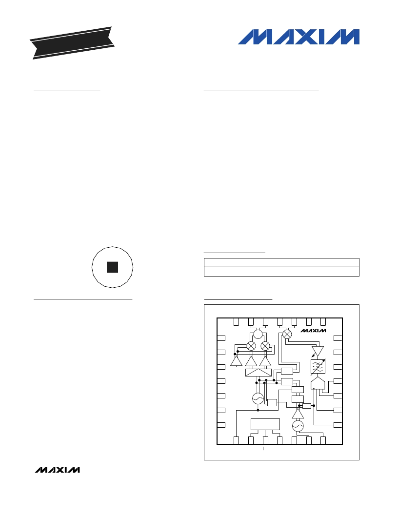
1
28
27
26
25
24
23
22
V
C
6
I
I
I
I
N
N
8
9
10
11
12
13
14
F
S
C
S
S
X
R
15
16
17
18
19
20
21
GPSCLK
GPSIF2
GPSIF1
GPSIF0
V
CC
5
N.C.
SDO
7
6
5
4
3
2
1
GND
V
CC
4
V
CC
3
VCO
3225.6MHz
V
CC
2
RFIN
N.C.
V
CC
1
Σ
LNA
1612.8MHz
33.6MHz
16.8MHz
200kHz
90
0
/96
/192
/2
/16128
P.D.
/R
REF
OSC
ADC
SPI INTERFACE
MAX2741
MUX
Pin Configuration/
Functional Diagram
Ordering Information
19-3559; Rev 0; 1/05
EVALUATION KIT
AVAILABLE
SPI is a trademark of Motorola, Inc.
PART
TEMP RANGE
-40°C to +85°C
PIN-PACKAGE
28 Thin QFN
MAX2741ETI
5
.
0
m
m
x
5
.
0
m
m
2
8
-
P
I
N
T
H
I
N
Q
F
N
相关PDF资料 |
PDF描述 |
|---|---|
| MAX2741ETI | Integrated L1-Band GPS Receiver |
| MAX2742 | Single-Chip Global Positioning System Receiver Front-End |
| MAX2742ECM | Single-Chip Global Positioning System Receiver Front-End |
| MAX2751 | 2.4GHz Monolithic Voltage-Controlled Oscillators |
| MAX2752 | CLAMP |
相关代理商/技术参数 |
参数描述 |
|---|---|
| MAX2741AETI+ | 功能描述:射频接收器 Integrated L1-Band GPS Receiver RoHS:否 制造商:Skyworks Solutions, Inc. 类型:GPS Receiver 封装 / 箱体:QFN-24 工作频率:4.092 MHz 工作电源电压:3.3 V 封装:Reel |
| MAX2741AETI+T | 功能描述:射频接收器 Integrated L1-Band GPS Receiver RoHS:否 制造商:Skyworks Solutions, Inc. 类型:GPS Receiver 封装 / 箱体:QFN-24 工作频率:4.092 MHz 工作电源电压:3.3 V 封装:Reel |
| MAX2741AEVKIT | 功能描述:GPS开发工具 MAX2741A Eval Kit RoHS:否 制造商:STMicroelectronics 产品:Evaluation Boards 工具用于评估:IT600, STM32F20x 频率:1.575 GHz 工作电源电压:1.8 V 接口类型:Wireless |
| MAX2741ETI | 功能描述:射频接收器 RoHS:否 制造商:Skyworks Solutions, Inc. 类型:GPS Receiver 封装 / 箱体:QFN-24 工作频率:4.092 MHz 工作电源电压:3.3 V 封装:Reel |
| MAX2741ETI+ | 功能描述:射频接收器 Integrated L1-Band GPS Receiver RoHS:否 制造商:Skyworks Solutions, Inc. 类型:GPS Receiver 封装 / 箱体:QFN-24 工作频率:4.092 MHz 工作电源电压:3.3 V 封装:Reel |
发布紧急采购,3分钟左右您将得到回复。