- 您现在的位置:买卖IC网 > PDF目录383349 > MAX2742 (Maxim Integrated Products, Inc.) Single-Chip Global Positioning System Receiver Front-End PDF资料下载
参数资料
| 型号: | MAX2742 |
| 厂商: | Maxim Integrated Products, Inc. |
| 英文描述: | Single-Chip Global Positioning System Receiver Front-End |
| 中文描述: | 单芯片、全球定位系统接收前端 |
| 文件页数: | 2/8页 |
| 文件大小: | 573K |
| 代理商: | MAX2742 |
M
Single-Chip Global Positioning System
Receiver Front-End
2
_______________________________________________________________________________________
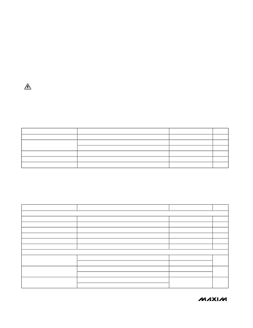
ABSOLUTE MAXIMUM RATINGS
V
DD
to GND...........................................................-0.3V to +3.7V
All Other Pins to GND.................................-0.3V to (V
DD
+ 0.3V)
RF LNA Input Power.......................................................+10dBm
Continuous Power Dissipation (T
A
= +70°C)
48-Pin TQFP-EP (derate 12.5mW/°C above +70°C)....100mW
DC ELECTRICAL CHARACTERISTICS
(MAX2742 EV kit, V
DD
= +2.4V to +3.6V, SHDN = V
DD
, T
A
= -40°C to +85°C. Typical values are at V
DD
= +3V and T
A
= +25°C,
unless otherwise noted.)
Stresses beyond those listed under “Absolute Maximum Ratings” may cause permanent damage to the device. These are stress ratings only, and functional
operation of the device at these or any other conditions beyond those indicated in the operational sections of the specifications is not implied. Exposure to
absolute maximum rating conditions for extended periods may affect device reliability.
Operating Temperature Range ...........................-40°C to +85°C
Junction Temperature......................................................+150°C
Storage Temperature Range.............................-65°C to +150°C
Soldering Temperature (10s)...........................................+300°C
PARAMETER
CONDITIONS
MIN
2.4
TYP
MAX
3.6
20
UNITS
V
mA
μA
V
V
μA
Supply Voltage
V
DD
= +3.0V, T
A
= +25
°
C (Note 1)
Shutdown mode
14
10
Supply Current
Logic-Input High Voltage
Logic-Input Low Voltage
Logic-Input Bias Current
V
DD
- 0.5
0.5
+40
-40
AC ELECTRICAL CHARACTERISTICS
(MAX2742 EV kit, V
DD
= +2.4V to +3.6V, SHDN = V
DD
, T
A
= -40
°
C to +85
°
C. Typical values are at V
DD
= +3V and T
A
= +25
°
C,
unless otherwise noted.)
PARAMETER
CONDITIONS
MIN
TYP
MAX
UNITS
GENERAL PERFORMANCE
Maximum Conversion Gain
Input Frequency
Noise Figure
Return Loss (S11)
LNA/Mixer Input IP3
Output IF Frequency
OUTPUT STAGE
(Notes 2, 3)
102
117
dB
MHz
dB
dB
dBm
MHz
1575.42
4.5
-15
-32
1.023
Measured at quantizer input
f
1
= 1.5MHz and f
2
= 2.0MHz above carrier frequency
Differential (VOUT+, VOUT-), C
L
< 20pF
Single ended (DOUT), C
L
< 20pF
Differential
Single ended
Differential
Single ended
25
5
Output Rise/Fall Time
ns
V
DD
- 0.9
0
Output-Voltage-Level Low
V
Output-Voltage-Level High
V
DD
V
CAUTION!
ESD SENSITIVE DEVICE
相关PDF资料 |
PDF描述 |
|---|---|
| MAX2742ECM | Single-Chip Global Positioning System Receiver Front-End |
| MAX2751 | 2.4GHz Monolithic Voltage-Controlled Oscillators |
| MAX2752 | CLAMP |
| MAX2751EUA | 2.4GHz Monolithic Voltage-Controlled Oscillators |
| MAX2750 | 2.4GHz Monolithic Voltage-Controlled Oscillators |
相关代理商/技术参数 |
参数描述 |
|---|---|
| MAX2742CCM | 功能描述:射频接收器 RoHS:否 制造商:Skyworks Solutions, Inc. 类型:GPS Receiver 封装 / 箱体:QFN-24 工作频率:4.092 MHz 工作电源电压:3.3 V 封装:Reel |
| MAX2742CCM+ | 功能描述:射频接收器 RoHS:否 制造商:Skyworks Solutions, Inc. 类型:GPS Receiver 封装 / 箱体:QFN-24 工作频率:4.092 MHz 工作电源电压:3.3 V 封装:Reel |
| MAX2742ECM | 功能描述:射频接收器 RoHS:否 制造商:Skyworks Solutions, Inc. 类型:GPS Receiver 封装 / 箱体:QFN-24 工作频率:4.092 MHz 工作电源电压:3.3 V 封装:Reel |
| MAX2742ECM+ | 功能描述:射频接收器 RoHS:否 制造商:Skyworks Solutions, Inc. 类型:GPS Receiver 封装 / 箱体:QFN-24 工作频率:4.092 MHz 工作电源电压:3.3 V 封装:Reel |
| MAX2742ECM+C0V | 功能描述:射频接收器 RoHS:否 制造商:Skyworks Solutions, Inc. 类型:GPS Receiver 封装 / 箱体:QFN-24 工作频率:4.092 MHz 工作电源电压:3.3 V 封装:Reel |
发布紧急采购,3分钟左右您将得到回复。