- 您现在的位置:买卖IC网 > PDF目录18821 > MAX2754EUA+T (Maxim Integrated)IC VCO 1.2GHZ W/MOD INPUT 8-UMAX PDF资料下载
参数资料
| 型号: | MAX2754EUA+T |
| 厂商: | Maxim Integrated |
| 文件页数: | 5/8页 |
| 文件大小: | 0K |
| 描述: | IC VCO 1.2GHZ W/MOD INPUT 8-UMAX |
| 标准包装: | 2,500 |
| 功能: | VCO |
| 频率: | 2.4GHz ~ 2.5GHz |
| RF 型: | 蓝牙 |
| 次要属性: | 线性调制输入 |
| 封装/外壳: | 8-TSSOP,8-MSOP(0.118",3.00mm 宽) |
| 包装: | 带卷 (TR) |
�� �
�
�1.2GHz� VCO� with� Linear�
�Modulation� Input�
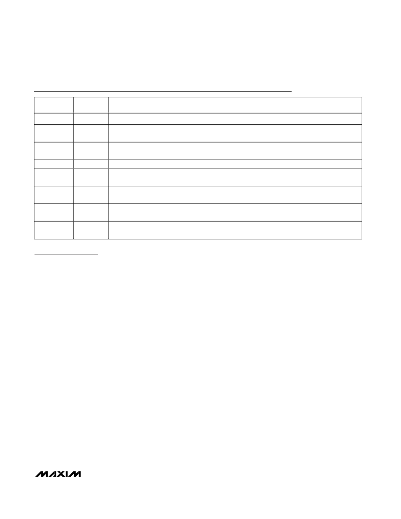
�Pin� Description�
�PIN�
�1�
�2�
�3�
�4�
�5�
�6�
�7�
�8�
�NAME�
�VREG�
�TUNE�
�GND1�
�MOD�
�SHDN�
�GND2�
�OUT�
�V� CC�
�FUNCTION�
�Capacitor� Connection� to� the� On-Chip� Linear� Regulator� Output.� Connect� a� 330nF� capacitor� to� ground.�
�Oscillator� Frequency� Tuning-Voltage� Input.� High-impedance� input� with� a� voltage� range� of� +0.4V� (low�
�frequency)� to� +2.4V� (high� frequency).�
�Ground� Connection� for� the� Oscillator� Core.� Requires� a� low-inductance� connection� to� the� circuit-�
�board� ground� plane.�
�Linear� Modulation� Input.� High-impedance� CMOS� input� with� a� voltage� range� of� +0.4V� to� +2.4V.�
�Shutdown� Input.� Drive� logic� low� to� place� the� device� in� shutdown� mode.� Drive� logic� high� for� normal�
�operation.�
�Ground� Connection� for� Output-Buffered� Amplifier,� Linear� Modulation� Interface,� and� Biasing.�
�Requires� a� low-inductance� connection� to� the� circuit-board� ground� plane.�
�Buffered� Oscillator� Output.� Incorporates� an� internal� DC-blocking� capacitor.� OUT� is� internally�
�matched� to� 50� ?� .�
�Supply� Voltage� Connection.� Requires� external� RF� bypass� capacitor� to� ground� for� low� noise� and� low�
�spurious� content� performance� from� the� oscillator.� Bypass� with� a� 330pF� capacitor� to� ground.�
�Detailed� Description�
�Oscillator�
�The� MAX2754� VCO� is� implemented� as� an� LC� oscillator�
�topology,� integrating� all� of� the� tank� components� on-�
�chip.� This� fully� monolithic� approach� provides� an�
�extremely� easy-to-use� VCO,� equivalent� to� a� VCO� mod-�
�ule.� The� frequency� is� controlled� by� a� voltage� applied� to�
�the� TUNE� pin.� The� VCO� core� uses� a� differential� topolo-�
�gy� to� provide� a� stable� frequency� versus� supply� voltage�
�and� improve� the� immunity� to� load� variations.� In� addi-�
�tion,� there� is� a� buffer� amplifier� following� the� oscillator�
�core� to� provide� added� isolation� from� load� and� supply�
�variations� and� to� boost� the� output� power.�
�Linear� Modulation�
�The� linear� modulation� input� offers� a� means� to� directly�
�FM� modulate� the� VCO� with� a� controlled� amount� of� fre-�
�quency� deviation� for� a� given� input� voltage� deviation.�
�The� unique� technique� maintains� a� consistent� modula-�
�tion� gain� (df/dV� MOD� )� across� the� entire� frequency� tuning�
�range� of� the� part,� enabling� accurate� FM� modulation�
�derived� solely� from� the� filtered� NRZ� “data”� stream� (the�
�modulation� voltage� input).�
�The� modulation� input� is� single-ended� and� centered�
�about� +1.4V.� The� linear� modulation� full-scale� range� is�
�±1V� around� this� point,� for� a� +0.4V� to� +2.4V� input� volt-�
�age� range.� A� very� important� point� to� note� is� that� the�
�sign� of� the� modulation� gain� is� negative.� A� positive�
�change� in� V� MOD� results� in� a� negative� change� in� oscilla-�
�tion� frequency.� This� convention� for� the� modulation� gain�
�is� due� to� the� practical� implementation� of� the� internal� lin-�
�earizing� circuitry.� This� gain� inversion� must� be� consid-�
�ered� when� designing� the� analog� voltage� interface� that�
�drives� the� linear� modulation� input.� The� easiest� way� to�
�handle� this� is� to� invert� the� logic� polarity� of� the� modula-�
�tion� data� three-state� output� buffer� (TX� data� output).�
�Where� it� is� impossible� to� invert� the� data-stream� logic�
�polarity,� an� external� inverter� and� three-state� buffer�
�would� be� required.� These� devices� are� offered� in� small�
�single-logic� gates� in� SC-79� style� packages� from� various�
�manufacturers� (e.g.,� Fairchild� —Tiny� Logic,� On�
�Semiconductor,� or� Rohm).�
�Figure� 1� illustrates� the� frequency� versus� V� MOD� charac-�
�teristic� of� the� modulation� input.� Note� the� negative� slope�
�of� the� curve,� df� MOD� /dV� MOD� <� 0,� where� f� MOD� =� f� OUT� -�
�f� NOM� .�
�Output� Buffer�
�The� oscillator� signal� from� the� core� drives� an� output�
�buffer� amplifier.� The� amplifier� is� internally� matched� to�
�50� ?� including� an� on-chip� DC-blocking� capacitor.� The�
�return� loss� can� be� improved� to� a� minimum� of� 12dB� over�
�1145MHz� to� 1250MHz� by� adding� a� 2.5nH� series� induc-�
�tor� and� a� 3.0pF� shunt� capacitor.� The� output� buffer� has�
�a� ground� connection� separate� from� the� oscillator� core�
�to� minimize� load-pulling� effects.� The� amplifier� boosts�
�the� oscillator� signal� to� a� level� suitable� for� driving� most�
�RF� mixers.�
�_______________________________________________________________________________________�
�5�
�相关PDF资料 |
PDF描述 |
|---|---|
| MAX1005CEE+T | IC UNDERSAMPLER IF 16-QSOP |
| MAX2014EUA+T | IC LOG DETECTR/CTRLR 8UMAX |
| MAX2750EUA+T | IC OSC VOLT CNTRL 8-UMAX |
| MAX2624EUA+T | IC SELF-CONTAINED VCO 8-UMAX |
| MAX2623EUA+T | IC SELF-CONTAINED VCO 8-MSOP |
相关代理商/技术参数 |
参数描述 |
|---|---|
| MAX2754EVKIT | 功能描述:时钟和定时器开发工具 RoHS:否 制造商:Texas Instruments 产品:Evaluation Modules 类型:Clock Conditioners 工具用于评估:LMK04100B 频率:122.8 MHz 工作电源电压:3.3 V |
| MAX2754EVKIT+ | 功能描述:时钟和定时器开发工具 MAX2754 Eval Kit RoHS:否 制造商:Texas Instruments 产品:Evaluation Modules 类型:Clock Conditioners 工具用于评估:LMK04100B 频率:122.8 MHz 工作电源电压:3.3 V |
| MAX275ACPP | 功能描述:有源滤波器 RoHS:否 制造商:Maxim Integrated 通道数量:1 截止频率:150 KHz 电源电压-最大:11 V 电源电压-最小:4.74 V 最大工作温度:+ 85 C 安装风格:Through Hole 封装 / 箱体:PDIP N 封装:Tube |
| MAX275ACPP+ | 功能描述:有源滤波器 4th & 8th Order Continuous-Time RoHS:否 制造商:Maxim Integrated 通道数量:1 截止频率:150 KHz 电源电压-最大:11 V 电源电压-最小:4.74 V 最大工作温度:+ 85 C 安装风格:Through Hole 封装 / 箱体:PDIP N 封装:Tube |
| MAX275ACWP | 功能描述:有源滤波器 RoHS:否 制造商:Maxim Integrated 通道数量:1 截止频率:150 KHz 电源电压-最大:11 V 电源电压-最小:4.74 V 最大工作温度:+ 85 C 安装风格:Through Hole 封装 / 箱体:PDIP N 封装:Tube |
发布紧急采购,3分钟左右您将得到回复。