- 您现在的位置:买卖IC网 > PDF目录9769 > MAX3162ECAI+T (Maxim Integrated Products)IC TXRX RS232/485/422 28SSOP PDF资料下载
参数资料
| 型号: | MAX3162ECAI+T |
| 厂商: | Maxim Integrated Products |
| 文件页数: | 12/23页 |
| 文件大小: | 0K |
| 描述: | IC TXRX RS232/485/422 28SSOP |
| 产品培训模块: | Lead (SnPb) Finish for COTS Obsolescence Mitigation Program |
| 标准包装: | 2,000 |
| 类型: | 收发器 |
| 驱动器/接收器数: | 2/2 |
| 规程: | RS232,RS422,RS485 |
| 电源电压: | 3 V ~ 5.5 V |
| 安装类型: | 表面贴装 |
| 封装/外壳: | 28-SSOP(0.209",5.30mm 宽) |
| 供应商设备封装: | 28-SSOP |
| 包装: | 带卷 (TR) |
+3.0V to+5.5V, 1A, RS-232/RS-485/422
Multiprotocol Transceivers
ABSOLUTE MAXIMUM RATINGS
ELECTRICAL CHARACTERISTICS
(VCC = +3V to +5.5V, C1–C4 = 0.1F when tested at +3.3V ±10%; C1 = 0.047F and C2, C3, C4 = 0.33F when tested at +5V
±10%; TA = TMIN to TMAX, unless otherwise noted. Typical values are at TA = +25°C.)
Stresses beyond those listed under “Absolute Maximum Ratings” may cause permanent damage to the device. These are stress ratings only, and functional
operation of the device at these or any other conditions beyond those indicated in the operational sections of the specifications is not implied. Exposure to
absolute maximum rating conditions for extended periods may affect device reliability.
Note 1: V+ and V- can have maximum magnitudes of 7V, but their absolute difference cannot exceed 13V.
VCC to GND. .............................................................-0.3V to +6V
V+ to GND ................................................................-0.3V to +7V
V- to GND....................................................................0.3V to -7V
V+ - V- (Note 1)....................................................................+13V
Input Voltages
T1IN, T2IN, DI, DE485, RE485, TE232, RE232, SHDN,
FAST, HDPLX, RS485/RS232 to GND. ...............-0.3V to +6V
A, B, R1IN, R2IN to GND ...............................................±25V
Output Voltages
T1OUT, T2OUT, Y, Z to GND......................................±13.2V
R2OUT, R1OUT, RO to GND................-0.3V to (VCC + 0.3V)
Output Short-Circuit Duration
T1OUT, T2OUT, Y, Z ............................................Continuous
Continuous Power Dissipation (TA = +70°C)
20-Pin SSOP (derate 11.9W/°C above +70°C) ..........952mW
24-Pin SSOP (derate 14.9W/°C above +70°C) ........1195mW
28-Pin SSOP (derate 15W/°C above +70°C) ...........1201mW
Operating Temperature Ranges
MAX316_CA_ ....................................................0°C to +70°C
MAX316_EA_ .................................................-40°C to +85°C
Storage Temperature Range .............................-65°C to +150°C
Junction Temperature ......................................................+150°C
Lead Temperature (soldering, 10s) .................................+300°C
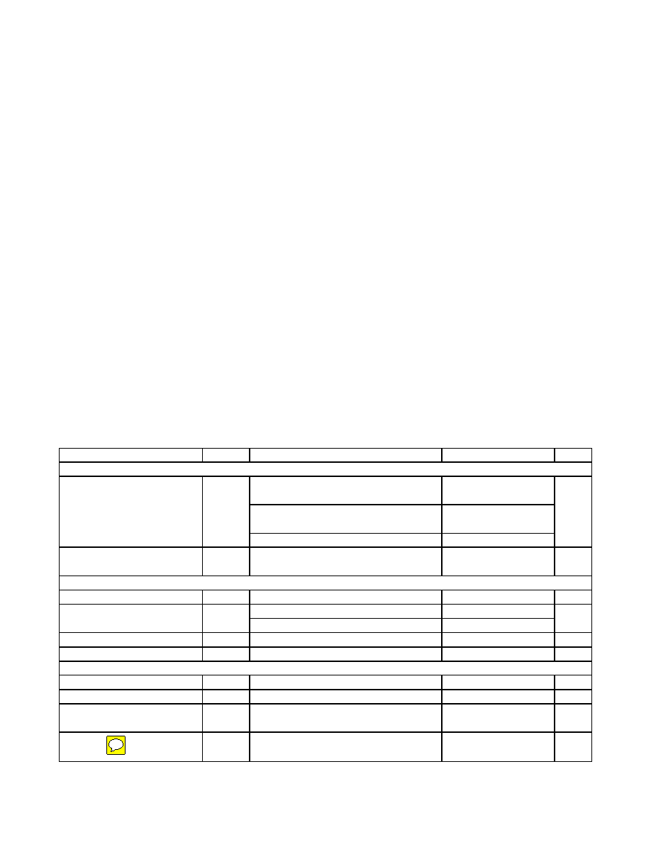
PARAMETER
SYMBOL
CONDITIONS
MIN
TYP
MAX
UNITS
DC CHARACTERISTICS
MAX3160/MAX3161, no load,
RS485/ RS232 = GND
1.2
2.5
MAX3160/MAX3161, no load,
RS485/ RS232 = VCC
2.5
5.5
VCC Standby Current
ICC
MAX3162 No Load
3.0
6
mA
VCC Shutdown Current
ICC
SHDN = GND, receiver inputs open or
grounded
110
A
TRANSMITTER AND LOGIC INPUTS (DI, T1IN, T2IN, DE485,
R
RE
E
E44
4
488
8
855
5
5, TE232, R
R
RE
E
E22
2
233
3
322
2
2, FAST, HDPLX, SHDN, RS485/R
R
RS
S
S22
2
233
3
322
2
2)
Logic Input Low
VIL
0.8
V
VCC = +3.3V
2.0
Logic Input High
VIH
VCC = +5V
2.4
V
Logic Input Leakage Current
IINL
±0.01
±1A
Transmitter Logic Hysteresis
VHYS
0.5
V
RS-232 AND RS-485/422 RECEIVER OUTPUTS (R1OUT, R2OUT, RO)
Receiver Output Voltage Low
VOL
IOUT = 2.5mA
0.4
V
Receiver Output Voltage High
VOH
IOUT = -1.5mA
VCC - 0.6
V
Receiver Output Short Circuit
Current
IOSR
0 < VO < VCC
±20
±60
mA
Receiver Output Leakage
Current
IOZR
Receivers disabled
±0.05
±1A
2
Maxim Integrated
MAX3160/MAX3161/MAX3162
相关PDF资料 |
PDF描述 |
|---|---|
| MAX3161ECAG+T | IC TXRX RS232/485/422 24SSOP |
| VE-B43-MW-F3 | CONVERTER MOD DC/DC 24V 100W |
| MAX3160ECAP+T | IC TXRX RS232/485/422 20SSOP |
| MS3100C28-9S | CONN RCPT 12POS WALL MNT W/SCKT |
| MAX3120EUA+ | IC TXRX INFRARED IRDA 8-UMAX |
相关代理商/技术参数 |
参数描述 |
|---|---|
| MAX3162EEAI | 功能描述:RS-422/RS-485 接口 IC RoHS:否 制造商:Maxim Integrated 数据速率:1136 Kbps 工作电源电压:3 V to 5.5 V 电源电流:5.9 mA 工作温度范围:- 40 C to + 85 C 安装风格:SMD/SMT 封装 / 箱体:SOIC-28 封装:Tube |
| MAX3162EEAI+ | 功能描述:RS-422/RS-485 接口 IC MAX3162EEAI+ RoHS:否 制造商:Maxim Integrated 数据速率:1136 Kbps 工作电源电压:3 V to 5.5 V 电源电流:5.9 mA 工作温度范围:- 40 C to + 85 C 安装风格:SMD/SMT 封装 / 箱体:SOIC-28 封装:Tube |
| MAX3162EEAI+T | 功能描述:RS-422/RS-485 接口 IC RoHS:否 制造商:Maxim Integrated 数据速率:1136 Kbps 工作电源电压:3 V to 5.5 V 电源电流:5.9 mA 工作温度范围:- 40 C to + 85 C 安装风格:SMD/SMT 封装 / 箱体:SOIC-28 封装:Tube |
| MAX3162EEAI-T | 功能描述:RS-422/RS-485 接口 IC RoHS:否 制造商:Maxim Integrated 数据速率:1136 Kbps 工作电源电压:3 V to 5.5 V 电源电流:5.9 mA 工作温度范围:- 40 C to + 85 C 安装风格:SMD/SMT 封装 / 箱体:SOIC-28 封装:Tube |
| MAX3162EEVKIT+ | 功能描述:RS-422/RS-485 接口 IC EVKits RoHS:否 制造商:Maxim Integrated 数据速率:1136 Kbps 工作电源电压:3 V to 5.5 V 电源电流:5.9 mA 工作温度范围:- 40 C to + 85 C 安装风格:SMD/SMT 封装 / 箱体:SOIC-28 封装:Tube |
发布紧急采购,3分钟左右您将得到回复。