- 您现在的位置:买卖IC网 > PDF目录1938 > MAX3170CAI (Maxim Integrated Products)IC TXRX CLOCK/DATA 3.3V 28-SSOP PDF资料下载
参数资料
| 型号: | MAX3170CAI |
| 厂商: | Maxim Integrated Products |
| 文件页数: | 9/16页 |
| 文件大小: | 0K |
| 描述: | IC TXRX CLOCK/DATA 3.3V 28-SSOP |
| 产品培训模块: | Lead (SnPb) Finish for COTS Obsolescence Mitigation Program |
| 标准包装: | 46 |
| 类型: | 收发器 |
| 驱动器/接收器数: | 3/3 |
| 规程: | RS232 |
| 电源电压: | 3 V ~ 3.6 V |
| 安装类型: | 表面贴装 |
| 封装/外壳: | 28-SSOP(0.209",5.30mm 宽) |
| 供应商设备封装: | 28-SSOP |
| 包装: | 管件 |
| 其它名称: | Q1162709A |
MAX3170
+3.3V, Multiprotocol, 3 Tx/3 Rx, Software-
Selectable Clock/Data Transceiver
2
_______________________________________________________________________________________
ABSOLUTE MAXIMUM RATINGS
ELECTRICAL CHARACTERISTICS
(VCC = +3.3V ±5%, C1 = C2 = 1F, C3 = C4 = 3.3F, TA = TMIN to TMAX, unless otherwise noted. Typical values are at TA = +25°C
and VCC = +3.3V.)
Stresses beyond those listed under “Absolute Maximum Ratings” may cause permanent damage to the device. These are stress ratings only, and functional
operation of the device at these or any other conditions beyond those indicated in the operational sections of the specifications is not implied. Exposure to
absolute maximum rating conditions for extended periods may affect device reliability.
Note 1: V+ and V- can have maximum magnitudes of 7V, but their absolute difference cannot exceed 13V.
(All voltages referenced to GND unless otherwise noted.)
Supply Voltages
VCC ......................................................................-0.3V to +4V
V+ (Note 1) ..........................................................-0.3V to +7V
V- (Note 1) ...........................................................+0.3V to -7V
V+ to V- (Note 1) ...............................................................13V
Logic Input Voltages
M0, M1, M2, DCE/DTE, T_IN ...............................-0.3V to +6V
Logic Output Voltages
R_OUT ...................................................-0.3V to (VCC + 0.3V)
Short-Circuit Duration............................................Continuous
Transmitter Outputs
T_OUT_...............................................................-15V to +15V
Short-Circuit Duration ........................................................60s
Receiver Inputs
R_IN_ ..................................................................-15V to +15V
Continuous Power Dissipation (TA = +70°C)
28-Pin SSOP (derate 11.1mW/°C above +70°C) ........889mW
Operating Temperature Range
MAX3170CAI .....................................................0°C to +70°C
Storage Temperature Range ............................-65°C to +150°C
Lead Temperature (soldering, 10s) ................................+300°C
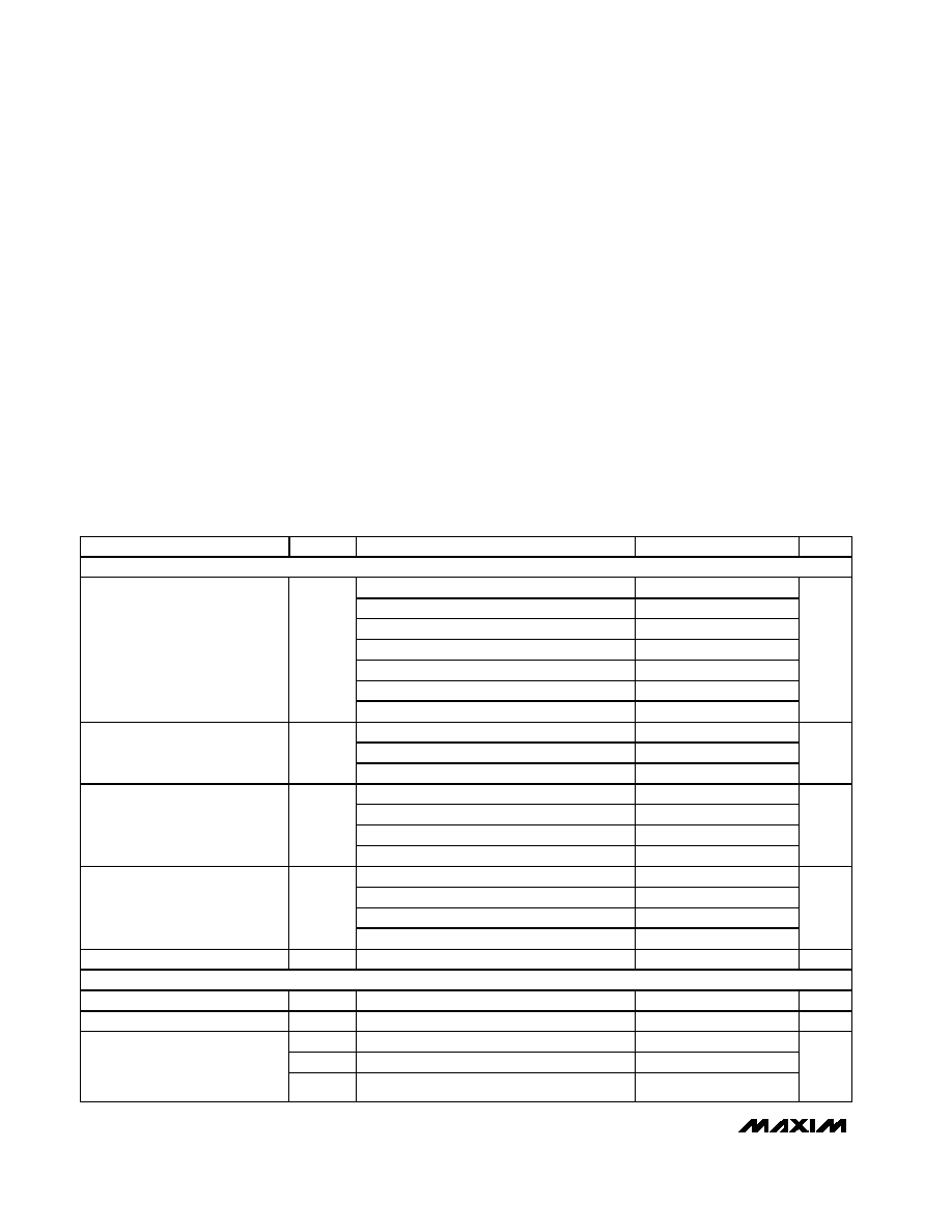
PARAMETER
SYMBOL
CONDITIONS
MIN
TYP
MAX
UNITS
DC CHARACTERISTICS
V.11 mode
190
250
V.11 mode with no load
3
7
V.35 mode
160
210
V.35 mode with no load
20
40
V.28 mode
10
20
V.28 mode with no load
4
7
Supply Current (DCE Mode)
(Digital Inputs = GND or VCC)
(All Outputs Static)
ICC
No-cable mode
0.8
2
mA
V.11 mode, full load
410
V.35 mode, full load
510
Internal Power Dissipation
(DCE Mode)
PD
V.28 mode, full load
15
mW
V.11 mode
4
V.35 mode
4.25
V.28 mode
5.55
V+ Output Voltage (DCE Mode)
(Full Load)
V+
No-cable mode
5
V
V.11 mode
-4.1
V.35 mode
-3.7
V.28 mode
-5.45
V- Output Voltage (DCE Mode)
(Full Load)
V-
No-cable mode
-4.25
V
Charge-Pump Enable Time
Delay until V+ and V- specifications met
1
ms
LOGIC INPUTS (M0, M1, M2, DCE/DTE, T_IN)
Input High Voltage
VIH
2.0
V
Input Low Voltage
VIL
0.8
V
IIN
T_IN
±1
IIH
M0, M1, M2, DCE/DTE = VCC
±1
Logic Input Current
IIL
M0, M1, M2, DCE/DTE = GND
30
50
100
A
相关PDF资料 |
PDF描述 |
|---|---|
| MAX3171CAI | IC TXRX MULTIPROTOCL 3.3V 28SSOP |
| MAX3172CAI | IC TXRX MULTIPROTOCL 3.3V 28SSOP |
| MAX3175CAI+ | IC TXRX MULTIPROTOCOL 28-SSOP |
| MAX31782ETL+T | IC MICROCONTROLLER 40TQFN |
| MAX3181EUK-T | IC RCVR RS232 1.5MBPS SOT23-5 |
相关代理商/技术参数 |
参数描述 |
|---|---|
| MAX3170CAI+ | 功能描述:接口 - 专用 3.3V 3Tx/3Rx Tcvr Multiprotocol RoHS:否 制造商:Texas Instruments 产品类型:1080p60 Image Sensor Receiver 工作电源电压:1.8 V 电源电流:89 mA 最大功率耗散: 最大工作温度:+ 85 C 安装风格:SMD/SMT 封装 / 箱体:BGA-59 |
| MAX3170CAI+T | 功能描述:接口 - 专用 3.3V 3Tx/3Rx Tcvr Multiprotocol RoHS:否 制造商:Texas Instruments 产品类型:1080p60 Image Sensor Receiver 工作电源电压:1.8 V 电源电流:89 mA 最大功率耗散: 最大工作温度:+ 85 C 安装风格:SMD/SMT 封装 / 箱体:BGA-59 |
| MAX3170CAI-T | 功能描述:RS-232接口集成电路 RoHS:否 制造商:Exar 数据速率:52 Mbps 工作电源电压:5 V 电源电流:300 mA 工作温度范围:- 40 C to + 85 C 安装风格:SMD/SMT 封装 / 箱体:LQFP-100 封装: |
| MAX3170EVKIT | 功能描述:RS-232接口集成电路 RoHS:否 制造商:Exar 数据速率:52 Mbps 工作电源电压:5 V 电源电流:300 mA 工作温度范围:- 40 C to + 85 C 安装风格:SMD/SMT 封装 / 箱体:LQFP-100 封装: |
| MAX3171CAI | 功能描述:RS-232接口集成电路 RoHS:否 制造商:Exar 数据速率:52 Mbps 工作电源电压:5 V 电源电流:300 mA 工作温度范围:- 40 C to + 85 C 安装风格:SMD/SMT 封装 / 箱体:LQFP-100 封装: |
发布紧急采购,3分钟左右您将得到回复。