- 您现在的位置:买卖IC网 > PDF目录296460 > MAX317EPA (MAXIM INTEGRATED PRODUCTS INC) Precision, CMOS Analog Switches PDF资料下载
参数资料
| 型号: | MAX317EPA |
| 厂商: | MAXIM INTEGRATED PRODUCTS INC |
| 元件分类: | 多路复用及模拟开关 |
| 英文描述: | Precision, CMOS Analog Switches |
| 中文描述: | 1-CHANNEL, SGL POLE SGL THROW SWITCH, PDIP8 |
| 封装: | 0.300 INCH, PLASTIC, DIP-8 |
| 文件页数: | 9/12页 |
| 文件大小: | 130K |
| 代理商: | MAX317EPA |
MAX317/MAX318/MAX319
Precision, CMOS Analog Switches
6
_______________________________________________________________________________________
PIN
NAME
FUNCTION
MAX317
MAX318
MAX319
1
COM
Analog-switch common terminal
2
—
N.C.
No connect — not internally connected
—
8
NO
Analog-switch normally open terminal
3
GND
Logic ground
4
V+
Analog-signal positive supply input
5
VL
Logic-level positive supply input
6
IN
Logic-level input
7
V-
Analog-signal negative supply input
8
—
2
NC
Analog-switch normally closed terminal
—
8
—
NO
Analog-switch normally open terminal
_______________________________________________________________________Pin Description
__________Applications Information
Operation with Supply Voltages
Other Than ±15V
The main limitation of supply voltages other than ±15V
is analog signal range reduction. The MAX317/
MAX318/MAX319 switches operate with bipolar sup-
plies of ±5V to ±20V. Typical Operating Characteristics
graphs show typical on resistance for ±15V, ±10V, and
±5V supplies. Switching times increase by a factor of
two
or
more
for
operation
at
±5V.
The
MAX317/MAX318/MAX319 can operate from unipolar
supplies of +10V to +30V. Both parts can also operate
from unbalanced supplies such as +24V and -5V.
Connect V- to 0V when operating with a single supply.
This means that VL must be connected to +5V to be
TTL compatible, or to V+ for CMOS logic input levels.
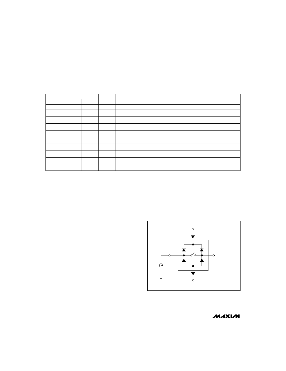
Overvoltage Protection
Proper power-supply sequencing is recommended for
all CMOS devices. It is important not to exceed the
absolute maximum ratings because stresses beyond
the listed ratings may cause permanent damage to the
devices. Always sequence V+ on first, followed by VL,
V-, and logic inputs. If power-supply sequencing is not
possible, protect the devices from overvoltage by
adding two small signal diodes in series with the sup-
ply pins (Figure 1). Adding the diodes reduces the
analog signal range to 1V below V+ and 1V below V-,
but low switch resistance and low leakage characteris-
tics are unaffected. Device operation is unchanged,
and the difference between V+ to V- should not exceed
+44V.
V+
COM_
V-
NO_
Vg
V+
V-
Figure 1. Overvoltage Protection Using Blocking Diodes
相关PDF资料 |
PDF描述 |
|---|---|
| MAX327ESE+T | Quad, SPST, Ultra-Low-Leakage, CMOS Analog Switches |
| MAX3317EEAP | 5V High-Speed RS-232 Transceivers with 0.1uF Capacitors |
| MAX379CPE | High-Voltage, Fault-Protected Analog Multiplexers |
| MAX3801UGG-T | 3.2Gbps Adaptive Equalizer |
| MAX4074AHESA-T | OP-AMP, 3500 uV OFFSET-MAX, 4 MHz BAND WIDTH, PDSO8 |
相关代理商/技术参数 |
参数描述 |
|---|---|
| MAX317EPA+ | 功能描述:模拟开关 IC Precision SPST NC CMOS RoHS:否 制造商:Texas Instruments 开关数量:2 开关配置:SPDT 开启电阻(最大值):0.1 Ohms 切换电压(最大): 开启时间(最大值): 关闭时间(最大值): 工作电源电压:2.7 V to 4.5 V 最大工作温度:+ 85 C 安装风格:SMD/SMT 封装 / 箱体:DSBGA-16 |
| MAX317ESA | 功能描述:模拟开关 IC RoHS:否 制造商:Texas Instruments 开关数量:2 开关配置:SPDT 开启电阻(最大值):0.1 Ohms 切换电压(最大): 开启时间(最大值): 关闭时间(最大值): 工作电源电压:2.7 V to 4.5 V 最大工作温度:+ 85 C 安装风格:SMD/SMT 封装 / 箱体:DSBGA-16 |
| MAX317ESA+ | 功能描述:模拟开关 IC Precision SPST NC CMOS RoHS:否 制造商:Texas Instruments 开关数量:2 开关配置:SPDT 开启电阻(最大值):0.1 Ohms 切换电压(最大): 开启时间(最大值): 关闭时间(最大值): 工作电源电压:2.7 V to 4.5 V 最大工作温度:+ 85 C 安装风格:SMD/SMT 封装 / 箱体:DSBGA-16 |
| MAX317ESA+T | 功能描述:模拟开关 IC Precision SPST NC CMOS RoHS:否 制造商:Texas Instruments 开关数量:2 开关配置:SPDT 开启电阻(最大值):0.1 Ohms 切换电压(最大): 开启时间(最大值): 关闭时间(最大值): 工作电源电压:2.7 V to 4.5 V 最大工作温度:+ 85 C 安装风格:SMD/SMT 封装 / 箱体:DSBGA-16 |
| MAX317ESA-T | 功能描述:模拟开关 IC RoHS:否 制造商:Texas Instruments 开关数量:2 开关配置:SPDT 开启电阻(最大值):0.1 Ohms 切换电压(最大): 开启时间(最大值): 关闭时间(最大值): 工作电源电压:2.7 V to 4.5 V 最大工作温度:+ 85 C 安装风格:SMD/SMT 封装 / 箱体:DSBGA-16 |
发布紧急采购,3分钟左右您将得到回复。