- 您现在的位置:买卖IC网 > PDF目录10669 > MAX3281EAUT+T (Maxim Integrated Products)IC RCVR RS485/422 SOT23-6 PDF资料下载
参数资料
| 型号: | MAX3281EAUT+T |
| 厂商: | Maxim Integrated Products |
| 文件页数: | 7/10页 |
| 文件大小: | 0K |
| 描述: | IC RCVR RS485/422 SOT23-6 |
| 产品培训模块: | Lead (SnPb) Finish for COTS Obsolescence Mitigation Program |
| 标准包装: | 1 |
| 类型: | 接收器 |
| 驱动器/接收器数: | 0/1 |
| 规程: | RS422,RS485 |
| 电源电压: | 3 V ~ 5.5 V |
| 安装类型: | 表面贴装 |
| 封装/外壳: | SOT-23-6 |
| 供应商设备封装: | SOT-6 |
| 包装: | 标准包装 |
| 其它名称: | MAX3281EAUT+TDKR |
6
Maxim Integrated
MAX3280E/MAX3281E/
MAX3283E/MAX3284E
±15kV ESD-Protected 52Mbps, 3V to 5.5V, SOT23
RS-485/RS-422 True Fail-Safe Receivers
users design equipment that meets Level 3 of IEC 1000-
4-2, without additional ESD-protection components.
The main difference between tests done using the
Human Body Model and IEC 1000-4-2 is higher peak
current in IEC 1000-4-2. Because series resistance is
lower in the IEC 1000-4-2 ESD test model (Figure 4a),
the ESD-withstand voltage measured to this standard is
generally lower than that measured using the Human
Body Model. Figure 4b shows the current waveform for
the ±8kV IEC 1000-4-2 Level 4 ESD Contact Discharge
test. The Air-Gap test involves approaching the device
with a charger probe. The Contact Discharge method
connects the probe to the device before the probe is
energized.
Machine Model
The Machine Model for ESD testing uses a 200pF stor-
age capacitor and zero-discharge resistance. It mimics
the stress caused by handling during manufacturing
and assembly. All pins (not just the RS-485 inputs)
require this protection during manufacturing. Therefore,
the Machine Model is less relevant to the I/O ports than
are the Human Body Model and IEC 1000-4-2.
True Fail-Safe
The MAX3280E/MAX3281E/MAX3283E/MAX3284E
guarantee a logic-high receiver output when the receiv-
er inputs are shorted or open, or when they are con-
nected to a terminated transmission line with all drivers
disabled. This guaranteed logic high is achieved by
setting the receiver threshold between -50mV and
-200mV. If the differential receiver input voltage
(VA - VB) is greater than or equal to -50mV, RO is logic
high. If (VA - VB) is less than or equal to -200mV, RO is
logic low.
In the case of a terminated bus with all transmitters dis-
abled, the receiver’s differential input voltage is pulled
to ground by the termination. This results in a logic high
with a 50mV minimum noise margin. Unlike previous
fail-safe devices, the -50mV to -200mV threshold com-
plies with the ±200mV EIA/TIA-485 standard.
Receiver Enable
(MAX3281E and MAX3283E only)
The MAX3281E and MAX3283E feature a receiver out-
put enable (EN, MAX3281E or EN, MAX3283E) input
that controls the receiver. The MAX3281E receiver
enable (EN) pin is active high, meaning the receiver
outputs are active when EN is high. The MAX3283E
receiver enable (EN) pin is active low. Receiver outputs
are high impedance when the MAX3281E’s EN pin is
low and when the MAX3283E’s EN pin is high.
Low-Voltage Logic Levels
(MAX3284E only)
An increasing number of applications now operate at
low-voltage logic levels. To enable compatibility with
these low-voltage logic level applications, such as digi-
tal FPGAs, the MAX3284E VL pin is a user-defined sup-
ply voltage that designates the voltage threshold for a
logic high.
At lower VL voltages, the data rate will also be lower. A
logic-high level of 1.65V will receive data at 20Mbps.
Table 2 gives data rates at various voltages at VL.
Applications Information
Propagation Delay Matching
The MAX3280E/MAX3281E/MAX3283E/MAX3284E
(VCC = VL) exhibit propagation delays that are closely
matched from one device to another, even between
devices from different production lots. This feature
allows multiple data lines to receive data and clock sig-
nals with minimal skew with respect to each other.
Figure 5 shows the typical propagation delays. Small
receiver skew times, the difference between the low-to-
high and high-to-low propagation delay, help maintain a
symmetrical ratio (50% duty cycle). The receiver skew
time | tPLH - tPHL | is under 2ns for either a 3.3V supply
or a 5V supply.
Multidrop Clock Distribution
Low package-to-package skew (8ns max) makes the
MAX3280E/MAX3281E/MAX3283E/MAX3284E
(VCC = VL) ideal for multidrop clock distribution. When
distributing a clock signal to multiple circuits over long
transmission lines, receivers in separate locations, and
possibly at two different temperatures, would ideally
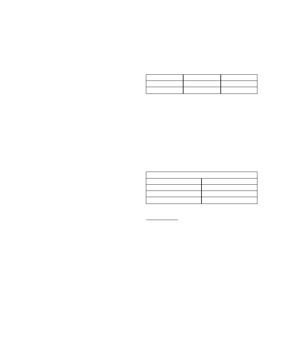
PART
ENABLE = HIGH
ENABLE = LOW
MAX3281E
Active
High Z
MAX3283E
High Z
Active
Table 1. MAX3281E/MAX3283E Enable
Table
VCC = 3V TO 5.5V
VL
MAXIMUM DATA RATE
1.65V
20Mbps
2.2V
33Mbps
≥3.3V
52Mbps
Table 2. MAX3284E Data Rate Table
相关PDF资料 |
PDF描述 |
|---|---|
| AD7738BRUZ | IC ADC 24BIT 8-CH 28-TSSOP |
| VE-J7T-MY-F1 | CONVERTER MOD DC/DC 6.5V 50W |
| AD7699BCPZ | IC ADC 8CH 16BIT 500KSPS 20LFCSP |
| ISL55141IRZ-T | IC COMP CMOS HS 18V 16-QFN |
| ISL55141IVZ-T | IC COMP CMOS HS 18V 14-TSSOP |
相关代理商/技术参数 |
参数描述 |
|---|---|
| MAX3283EAUT | 制造商:Maxim Integrated Products 功能描述:+/-15KV ESD-PROTECTED 52MBPS 3V TO - Bulk |
| MAX3283EAUT+ | 制造商:Maxim Integrated Products 功能描述:LINE RCVR 1RX 6PIN SOT-23 - Rail/Tube |
| MAX3283EAUT+T | 功能描述:RS-422/RS-485 接口 IC 52Mbps 3-5.5V RS-485 422 Fail Safe Rcvr RoHS:否 制造商:Maxim Integrated 数据速率:1136 Kbps 工作电源电压:3 V to 5.5 V 电源电流:5.9 mA 工作温度范围:- 40 C to + 85 C 安装风格:SMD/SMT 封装 / 箱体:SOIC-28 封装:Tube |
| MAX3283EAUT-T | 功能描述:RS-422/RS-485 接口 IC RoHS:否 制造商:Maxim Integrated 数据速率:1136 Kbps 工作电源电压:3 V to 5.5 V 电源电流:5.9 mA 工作温度范围:- 40 C to + 85 C 安装风格:SMD/SMT 封装 / 箱体:SOIC-28 封装:Tube |
| MAX3284EAUT | 制造商:Maxim Integrated Products 功能描述:+/-15KV ESD-PROTECTED 52MBPS 3V TO - Cut Tape Product |
发布紧急采购,3分钟左右您将得到回复。