- 您现在的位置:买卖IC网 > PDF目录10660 > MAX3295AUT+T (Maxim Integrated Products)IC TX RS485/422 DIFF SGL SOT23-6 PDF资料下载
参数资料
| 型号: | MAX3295AUT+T |
| 厂商: | Maxim Integrated Products |
| 文件页数: | 10/11页 |
| 文件大小: | 0K |
| 描述: | IC TX RS485/422 DIFF SGL SOT23-6 |
| 产品培训模块: | Lead (SnPb) Finish for COTS Obsolescence Mitigation Program |
| 标准包装: | 1 |
| 类型: | 收发器 |
| 驱动器/接收器数: | 1/0 |
| 规程: | RS422,RS485 |
| 电源电压: | 3.14 V ~ 3.47 V |
| 安装类型: | 表面贴装 |
| 封装/外壳: | SOT-23-6 |
| 供应商设备封装: | SOT-6 |
| 包装: | 标准包装 |
| 其它名称: | MAX3295AUT+TDKR |
MAX3293/MAX3294/MAX3295
20Mbps, +3.3V, SOT23 RS-485/
RS-422 Transmitters
8
_______________________________________________________________________________________
Detailed Description
The MAX3293/MAX3294/MAX3295 are low-power
transmitters for RS-485/RS-422 communication. The
MAX3295 operates at data rates up to 20Mbps, the
MAX3294 up to 2.5Mbps (slew-rate limited), and the
MAX3293 up to 250kbps (slew-rate limited). These
devices are enabled using an active-high driver enable
(DE) input. When disabled, outputs enter a high-imped-
ance state, and the supply current reduces to 1A.
The MAX3293/MAX3294/MAX3295 have a hot-swap
input structure that prevents disturbance on the differ-
ential signal lines when a circuit board is plugged into
a “hot” backplane (see the
Hot-Swap Capability sec-
tion). Drivers are also short-circuit current limited and
are protected against excessive power dissipation by
thermal-shutdown circuitry.
Driver
The driver accepts a single-ended, logic-level input
(DI) and translates it to a differential RS-485/RS-422
level output (Y and Z). Driving DE high enables the dri-
ver, while pulling DE low places the driver outputs
(Y and Z) into a high-impedance state (see Table 1).
Low-Power Shutdown
Force DE low to disable the MAX3293/MAX3294/
MAX3295. In shutdown mode, the device consumes a
maximum of 10A of supply current.
Hot-Swap Capability
Hot-Swap Input
When circuit boards are inserted into a “hot” or pow-
ered backplane, disturbances to the enable can lead to
data errors. Upon initial circuit board insertion, the
processor undergoes its power-up sequence. During
this period, the output drivers are high impedance and
are unable to drive the DE input of the MAX3293/
MAX3294/MAX3295 to a defined logic level. Leakage
currents up to 10A from the high-impedance output
could cause DE to drift to an incorrect logic state.
Additionally, parasitic circuit board capacitance could
cause coupling of VCC or GND to DE. These factors
could improperly enable the driver.
The MAX3293/MAX3294/MAX3295 eliminate all above
issues with hot-swap circuitry. When VCC rises, an
internal pulldown circuit holds DE low for approximately
10s. After the initial power-up sequence, the pulldown
circuit becomes transparent, resetting the hot-swap tol-
erable input.
Table 1. MAX3293/MAX3294/
MAX3295 (RS-485/RS-422) Transmitting
Function Table
X = Don’t care.
INPUTS
OUTPUTS
DE
DI
Y
Z
0
X
Shutdown
1001
1110
VCC
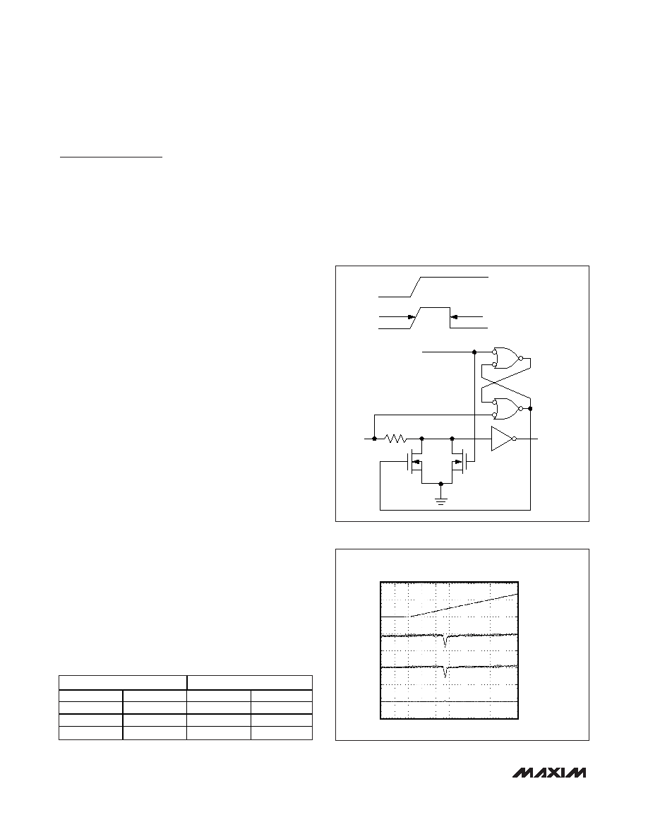
TIMER
EN
DE
(HOT SWAP)
10
μs
100
μA
M1
M2
5.6k
Ω
2mA
Figure 6. Simplified Structure of the Driver Enable Input (DE)
Figure 7. Differential Power-Up Glitch (0.1V/s)
DIFFERENTIAL POWER-UP GLITCH
(0.1V/
μs)
4
μs/div
2V/div
VCC
Y
Z
Y-Z
0V
10mV/div
AC-COUPLED
10mV/div
AC-COUPLED
20mV/div
相关PDF资料 |
PDF描述 |
|---|---|
| VE-J1L-MW-F3 | CONVERTER MOD DC/DC 28V 100W |
| LTC1414CGN#PBF | IC A/D CONV 14BIT SAMPLNG 28SSOP |
| VE-J1L-MW-F2 | CONVERTER MOD DC/DC 28V 100W |
| AD7664ASTZ | IC ADC 16BIT UNIPOLAR 48-LQFP |
| VE-J1L-MW-F1 | CONVERTER MOD DC/DC 28V 100W |
相关代理商/技术参数 |
参数描述 |
|---|---|
| MAX3296C/D | 功能描述:激光驱动器 3.0V to 5.5V 1.25Gbps/2.5Gbps LAN 激光驱动器 RoHS:否 制造商:Micrel 数据速率:4.25 Gbps 工作电源电压:3 V to 3.6 V 电源电流:80 mA 最大工作温度:+ 85 C 封装 / 箱体:QFN-16 封装:Tube |
| MAX3296C/D DIE | 制造商:Maxim Integrated Products 功能描述: |
| MAX3296C/D-B50041 WAF | 制造商:Maxim Integrated Products 功能描述: |
| MAX3296CGI | 功能描述:激光驱动器 3.0V - 5.5V 1.25Gbp LAN Laser Driver RoHS:否 制造商:Micrel 数据速率:4.25 Gbps 工作电源电压:3 V to 3.6 V 电源电流:80 mA 最大工作温度:+ 85 C 封装 / 箱体:QFN-16 封装:Tube |
| MAX3296CGILEVKIT | 功能描述:电源管理IC开发工具 RoHS:否 制造商:Maxim Integrated 产品:Evaluation Kits 类型:Battery Management 工具用于评估:MAX17710GB 输入电压: 输出电压:1.8 V |
发布紧急采购,3分钟左右您将得到回复。