- 您现在的位置:买卖IC网 > PDF目录1939 > MAX3349EETE+ (Maxim Integrated Products)IC TXRX USB 2.0 FS 16-TQFN PDF资料下载
参数资料
| 型号: | MAX3349EETE+ |
| 厂商: | Maxim Integrated Products |
| 文件页数: | 3/16页 |
| 文件大小: | 0K |
| 描述: | IC TXRX USB 2.0 FS 16-TQFN |
| 标准包装: | 75 |
| 类型: | 收发器 |
| 驱动器/接收器数: | 1/1 |
| 规程: | USB 2.0 |
| 电源电压: | 4 V ~ 5.5 V |
| 安装类型: | 表面贴装 |
| 封装/外壳: | 16-TQFN 裸露焊盘 |
| 供应商设备封装: | 16-TQFN-EP(4x4) |
| 包装: | 管件 |
MAX3349E
Hi-Speed USB 2.0 Full-Speed Transceiver
with UART Multiplexing Mode
______________________________________________________________________________________
11
USB Mode
The MAX3349E is in USB mode when VBUS is greater
than VTH-BUS and the bus detect output (BD) is logic-
high. In USB mode, power for the MAX3349E is derived
from VBUS, typically provided through the USB connec-
tor. An internal linear regulator generates the required
+3.3V VTRM voltage from VBUS. VTRM powers the inter-
nal USB transceiver circuitry and the D+ enumeration
resistor. Bypass VTRM to GND with a 1F ceramic
capacitor as close to the device as possible. Do not
power external circuitry from VTRM.
Disable Mode
Connect VBUS to a system power supply and leave VL
unconnected or connect to ground to enter disable
mode. In disable mode, D+ and D- are high imped-
ance, and withstand external signals up to +5.5V. OE,
SUS, and control signals are ignored.
UART Mode
Connect VL and VUART to system power supplies, and
leave VBUS unconnected or below VTH-BUS to operate
the MAX3349E in UART mode. The MAX3349E sup-
ports VUART from +2.7V to +3.3V (see Table 1).
USB Control Signals
OE
OE controls the direction of communication for USB
mode. When OE is logic-low, VP and VM operate as
logic inputs, and D+/D- are outputs. When OE is logic-
high, VP and VM operate as logic outputs, and D+/D-
are inputs. RCV is the output of the differential USB
receiver connected to D+/D-, and is not affected by the
OE logic level.
ENUM
Drive ENUM logic-high to enable the internal 1.5k
pullup resistor from D+ to VTRM. Drive ENUM logic-low
to disable the internal pullup resistor and logically dis-
connect the MAX3349E from the USB.
SUS
Operate the MAX3349E in low-power USB suspend
mode by driving SUS logic-high. In suspend mode, the
USB differential receiver is turned off and VBUS con-
sumes 38A (typ) of supply current. The single-ended
VP and VM receivers remain active to detect a SE0
state on USB bus lines D+ and D-. The USB transmitter
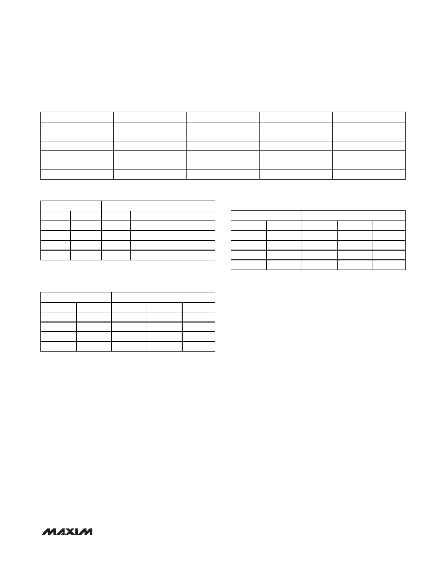
Table 1. Power-Supply Configuration
INPUTS
OUTPUTS
VP
VM
D+
D-
00
0
01
0
1
10
1
0
11
1
Table 2. USB Transmit Truth Table (OE = 0)
INPUTS
OUTPUTS
D+
D-
VP
VM
RCV
0000
RCV*
0101
0
1010
1
1111X
Table 3a. USB Receive Truth Table (OE = 1,
SUS = 0)
INPUTS
OUTPUTS
D+
D-
VP
VM
RCV
0000
0
0101
0
1010
0
1111
0
Table 3b. USB Receive Truth Table (OE = 1,
SUS = 1)
*
= Last State
X = Undefined
VBUS(V)
VTRM(V)
VL(V)
VUART(V)
CONFIGURATION
+4.0 to +5.5
+3.0 to +3.6 Output
+1.4 to +2.75
GND, Unconnected, or
+2.7V to +3.3V
USB Mode
+3.0 to +5.5
+2.8 to +3.6
+1.4 to +2.75
GND or Unconnected
Battery Mode
+4.0 to +5.5
+3.0 to +3.6 Output
GND or Unconnected
GND, Unconnected, or
+2.7V to +3.3V
Disable Mode
GND or Unconnected
High Impedance
+1.4 to +2.75
+2.7V to +3.3V
UART Mode
相关PDF资料 |
PDF描述 |
|---|---|
| MAX334EWE | IC SWITCH QUAD SPST 16SOIC |
| MAX335EWG | IC SWITCH OCTAL SPST 24SOIC |
| MAX3362AKA#TG16 | IC TXRX RS485/422 SGL SOT23-8 |
| MAX336CWI | IC MULTIPLEXER 16X1 28SOIC |
| MAX3380EEUP+T | IC TXRX RS232 460KBPS 20-TSSOP |
相关代理商/技术参数 |
参数描述 |
|---|---|
| MAX3349EETE+ | 功能描述:IC TXRX USB 2.0 FS 16-TQFN RoHS:是 类别:集成电路 (IC) >> 接口 - 驱动器,接收器,收发器 系列:- 产品培训模块:Lead (SnPb) Finish for COTS Obsolescence Mitigation Program 标准包装:25 系列:- 类型:收发器 驱动器/接收器数:2/2 规程:RS232 电源电压:4.5 V ~ 5.5 V 安装类型:通孔 封装/外壳:16-DIP(0.300",7.62mm) 供应商设备封装:16-PDIP 包装:管件 |
| MAX3349EETE+T | 制造商:Maxim Integrated Products 功能描述:USB TRNSCVR 1TX 1RX 12MBPS 16TQFN EP - Tape and Reel |
| MAX334C/D | 制造商:Maxim Integrated Products 功能描述: |
| MAX334CJE | 功能描述:模拟开关 IC RoHS:否 制造商:Texas Instruments 开关数量:2 开关配置:SPDT 开启电阻(最大值):0.1 Ohms 切换电压(最大): 开启时间(最大值): 关闭时间(最大值): 工作电源电压:2.7 V to 4.5 V 最大工作温度:+ 85 C 安装风格:SMD/SMT 封装 / 箱体:DSBGA-16 |
| MAX334CPE | 功能描述:模拟开关 IC RoHS:否 制造商:Texas Instruments 开关数量:2 开关配置:SPDT 开启电阻(最大值):0.1 Ohms 切换电压(最大): 开启时间(最大值): 关闭时间(最大值): 工作电源电压:2.7 V to 4.5 V 最大工作温度:+ 85 C 安装风格:SMD/SMT 封装 / 箱体:DSBGA-16 |
发布紧急采购,3分钟左右您将得到回复。