- 您现在的位置:买卖IC网 > PDF目录11124 > MAX335EWG+T (Maxim Integrated Products)IC SWITCH OCTAL SPST 24SOIC PDF资料下载
参数资料
| 型号: | MAX335EWG+T |
| 厂商: | Maxim Integrated Products |
| 文件页数: | 6/13页 |
| 文件大小: | 0K |
| 描述: | IC SWITCH OCTAL SPST 24SOIC |
| 产品培训模块: | Lead (SnPb) Finish for COTS Obsolescence Mitigation Program |
| 标准包装: | 1,000 |
| 功能: | 开关 |
| 电路: | 8 x SPST - NO |
| 导通状态电阻: | 150 欧姆 |
| 电压电源: | 双电源 |
| 电压 - 电源,单路/双路(±): | ±4.5 V ~ 20 V |
| 工作温度: | -40°C ~ 85°C |
| 安装类型: | 表面贴装 |
| 封装/外壳: | 24-SOIC(0.295",7.50mm 宽) |
| 供应商设备封装: | 24-SOIC W |
| 包装: | 带卷 (TR) |
MAX335
Serial Controlled, 8-Channel SPST Switch
2
_______________________________________________________________________________________
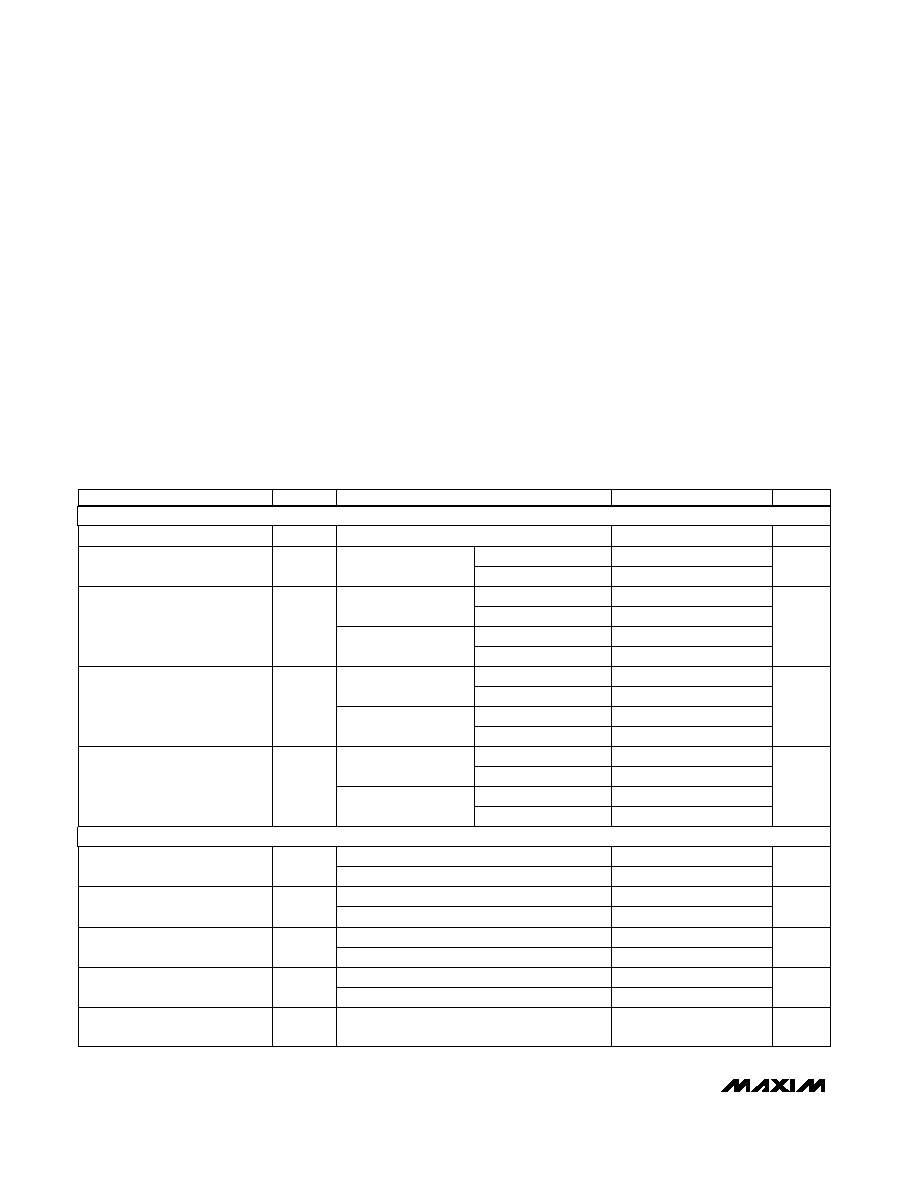
ABSOLUTE MAXIMUM RATINGS
ELECTRICAL CHARACTERISTICS
(VL = +5V ±10%, V+ = 15V, V- = -15V, TA = TMIN to TMAX, unless otherwise noted. Typical values are at TA = +25°C.)
Stresses beyond those listed under “Absolute Maximum Ratings” may cause permanent damage to the device. These are stress ratings only, and functional
operation of the device at these or any other conditions beyond those indicated in the operational sections of the specifications is not implied. Exposure to
absolute maximum rating conditions for extended periods may affect device reliability.
PARAMETER
SYMBOL
MIN
TYP
MAX
UNITS
-1
0.002
1
-20
20
-1
0.002
1
On-Resistance
RON
200
NO Off-Leakage Current
INO(OFF)
-20
20
nA
-1
0.002
1
-20
20
-1
0.002
1
Analog Signal Range
VANALOG
-15
15
V
100
150
COM Off-Leakage Current
ICOM(OFF)
-20
20
nA
-2
0.01
2
-40
40
-2
0.01
2
COM On-Leakage Current
ICOM(ON)
-40
40
nA
2.4
DIN, SCLK,
CS Input Logic
Threshold High
VIH
11
V
0.8
DIN, SCLK,
–
CS Input Logic
Threshold Low
VIL
3
V
-1
0.03
1
DIN, SCLK,
CS Input Current
Logic High
-1
0.03
1
A
IINH
CONDITIONS
VCOM = -14V,
VNO = +14V
VCOM = -14V,
VNO = +14V
VCOM = ±10V,
INO = 1mA
VCOM = -14V,
VNO = +14V
VCOM = VNO = +14V
VCOM = -14V,
VNO = +14V
VCOM = VNO = -14V
TA = TMIN to TMAX
VDIN, VSCLK, VCS = 2.4V
VL = +15V, VDIN, VSCLK, V
–
C
—
S
– = 11V
TA = +25°C
DIN, SCLK,
–
CS Input Current
Logic Low
IINL
VDIN, VSCLK, VCS = 0.8V
-1
0.03
1
A
DOUT Output Voltage
Logic High
VDOUT
IDOUT = 0.8mA
3.5
VL
V
TA = +25°C
VL = +5V
VL = +15V
VL = +5V
VL = +15V
VL = +15V, VDIN, VSCLK, V
–
C
—
S
– = 3V
-1
0.03
1
SWITCH
DIGITAL I/O
TA = +25°C
Note 1:
All leads are soldered or welded to PC boards.
Voltages Referenced to V-
V+...........................................................................................44V
GND .......................................................................................25V
VL .....................................................(GND - 0.3V) to (V+ + 0.3V)
SCLK, CS, DIN, DOUT, NO_, COM_ ...............V- -2V to V+ +2V
or 30mA, whichever occurs first
Continuous Current (any terminal) .......................................30mA
Peak Current, NO or COM
(pulsed at 1ms, 10% duty cycle MAX) ...............................00mA
Continuous Power Dissipation (TA = +70°C) (Note 1)
Narrow Plastic DIP (derate 13.33mW/°C above +70°C)1067mW
Wide SO (derate 11.76mW/°C above +70°C) .................941mW
Narrow CERDIP (derate 12.50mW/°C above +70°C) .....1000mW
TSSOP (derate 12.2mW/°C above +70°C)...........................30mA
Operating Temperature Ranges
MAX335C_ _ ............................................................0°C to +70°C
MAX335E_ _ .........................................................-40°C to +85°C
MAX335MRG.......................................................-55°C to +125°C
Storage Temperature Range ..............................-65°C to +160°C
Lead Temperature (soldering, 10sec)...............................+300°C
相关PDF资料 |
PDF描述 |
|---|---|
| MAX351CSE+T | IC SWITCH QUAD SPST 16SOIC |
| MAX352CSE+T | IC SWITCH QUAD SPST 16SOIC |
| MAX353CSE+T | IC SWITCH QUAD SPST 16SOIC |
| VE-2W4-IY-F4 | CONVERTER MOD DC/DC 48V 50W |
| MAX4533CAP+T | IC SWITCH QUAD SPDT 20SSOP |
相关代理商/技术参数 |
参数描述 |
|---|---|
| MAX335MRG | 功能描述:模拟开关 IC RoHS:否 制造商:Texas Instruments 开关数量:2 开关配置:SPDT 开启电阻(最大值):0.1 Ohms 切换电压(最大): 开启时间(最大值): 关闭时间(最大值): 工作电源电压:2.7 V to 4.5 V 最大工作温度:+ 85 C 安装风格:SMD/SMT 封装 / 箱体:DSBGA-16 |
| MAX3362AKA | 制造商:Maxim Integrated Products 功能描述:3.3V, HIGH-SPEED, RS-485/RS-422 TRANSCEIVER I - Bulk |
| MAX3362AKA#G16 | 制造商:Maxim Integrated Products 功能描述:3.3V, HIGH-SPEED, RS-485/RS-422 TRA - Rail/Tube |
| MAX3362AKA#TG16 | 功能描述:RS-422/RS-485 接口 IC 3.3V High-Speed Transceiver RoHS:否 制造商:Maxim Integrated 数据速率:1136 Kbps 工作电源电压:3 V to 5.5 V 电源电流:5.9 mA 工作温度范围:- 40 C to + 85 C 安装风格:SMD/SMT 封装 / 箱体:SOIC-28 封装:Tube |
| MAX3362AKA/GH9 | 制造商:Maxim Integrated Products 功能描述:- Rail/Tube |
发布紧急采购,3分钟左右您将得到回复。